
Datasheet

Section 12 Serial Communication Interface
Rev.7.00 Dec. 24, 2008 Page 406 of 698
REJ09B0074-0700
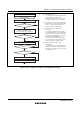
Note: * Figure 12.6 shows an example when the ABCS bit of SEMRA_0 is cleared to 0. When
ABCS is set to 1, the clock frequency of basic clock is 8 times the bit rate and the
receive data is sampled at the rising edge of the 4th pulse of the basic clock.
12.4.3 Clock
Either an internal clock generated by the on-chip baud rate generator or an external clock input at
the SCK pin can be selected as the SCI's serial clock, according to the setting of the C/A bit in
SMR and the CKE0 and CKE1 bits in SCR. When an external clock is input at the SCK pin, the
clock frequency should be 16 times the bit rate used. When an external clock is selected, the basic
clock of average transfer rate can be selected according to the ACS2 to ACS0 bit setting of
SEMR_0.
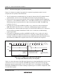
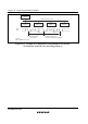
When the SCI is operated on an internal clock, the clock can be output from the SCK pin by
setting CKE1 = 0 and CKE0 = 1. The frequency of the clock output in this case is equal to the bit
rate, and the phase is such that the rising edge of the clock is in the middle of the transmit data, as
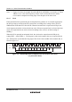
shown in figure 12.7.
0
1 frame
D0 D1 D2 D3 D4 D5 D6 D7 0/1
11
SCK
TxD
Figure 12.7 Relationship between Output Clock and Transfer Data Phase
(Asynchronous Mode)