
Datasheet

Section 12 Serial Communication Interface
Rev.7.00 Dec. 24, 2008 Page 420 of 698
REJ09B0074-0700
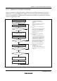
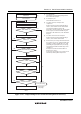
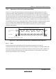
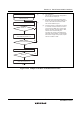
12.6.2 SCI Initialization (Clocked Synchronous Mode)
Before transmitting and receiving data, the TE and RE bits in SCR should be cleared to 0, then the
SCI should be initialized as described in a sample flowchart in figure 12.18. When the operating
mode, or transfer format, is changed for example, the TE and RE bits must be cleared to 0 before
making the change using the following procedure. When the TE bit is cleared to 0, the TDRE flag
is set to 1. Note that clearing the RE bit to 0 does not change the contents of the RDRF, PER,
FER, and ORER flags, or the contents of RDR.
Wait
<Transfer start>
Start initialization
Set data transfer format in
SMR and SCMR
No
Yes
Set value in BRR
Clear TE and RE bits in SCR to 0
[2]
[3]
Set TE and RE bits in SCR to 1, and
set RIE, TIE, TEIE, and MPIE bits
[4]
1-bit interval elapsed?
Set CKE1 and CKE0 bits in SCR
(TE, RE bits 0)
[1]
[1] Set the clock selection in SCR. Be sure to
clear bits RIE, TIE, TEIE, and MPIE, TE and
RE, to 0.
[2] Set the data transfer format in SMR and
SCMR.
[3] Write a value corresponding to the bit rate to
BRR. Not necessary if an external clock is
used.
[4] Wait at least one bit interval, then set the TE
bit or RE bit in SCR to 1.
Also set the RIE, TIE TEIE, and MPIE bits.
Setting the TE and RE bits enables the TxD
and RxD pins to be used.
Note: In simultaneous transmit and receive operations, the TE and RE bits should both be cleared
to 0 or set to 1 simultaneously.
Figure 12.18 Sample SCI Initialization Flowchart