
Datasheet

Section 15 A/D Converter
Rev.7.00 Dec. 24, 2008 Page 544 of 698
REJ09B0074-0700
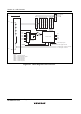
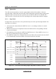
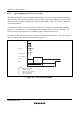
15.5.3 Input Sampling and A/D Conversion Time
The A/D converter has a built-in sample-and-hold circuit. The A/D converter samples the analog
input when the A/D conversion start delay time (t
D
) has passed after the ADST bit is set to 1, then
starts conversion. Figure 15.5 shows the A/D conversion timing. Tables 15.3 and 15.4 show the
A/D conversion time.
As indicated in figure 15.5, the A/D conversion time (t
CONV
) includes t
D
and the input sampling
time (t
SPL
). The length of t
D
varies depending on the timing of the write access to ADCSR. The
total conversion time therefore varies within the ranges indicated in table 15.4.
In scan mode, the values given in table 15.4 apply to the first conversion time. The values given in
table 15.3 apply to the second and subsequent conversions.
(1)
(2)
t
D
t
SPL
t
CONV
φ
A
ddress
Write signal
Input sampling
timing
A
DF
Legend:
(1): ADCSR write cycle
(2): ADCSR address
t
D
: A/D conversion start delay
t
SPL
: Input sampling time
t
CONV
:
A/D conversion time
Figure 15.5 A/D Conversion Timing