
Datasheet

Section 19 Clock Pulse Generator
Rev.7.00 Dec. 24, 2008 Page 605 of 698
REJ09B0074-0700
19.9 Usage Notes
19.9.1 Note on Crystal Resonator
Since various characteristics related to the crystal resonator are closely linked to the user's board
design, thorough evaluation is necessary on the user's part, using the resonator connection
examples shown in this section as a guide. As the resonator circuit ratings will depend on the
floating capacitance of the resonator and the mounting circuit, the ratings should be determined in
consultation with the resonator manufacturer. The design must ensure that a voltage exceeding the
maximum rating is not applied to the oscillator pin.
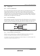
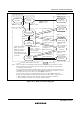
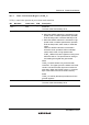
19.9.2 Note on Board Design
When designing the board, place the crystal resonator and its load capacitors as close as possible to
the XTAL or OSC1 and EXTAL or OSC2 pins. Other signal lines should be routed away from the
oscillator circuit to prevent induction from interfering with correct oscillation. See figure 19.10.
Prohibit
Signal A Signal B
This LSI
EXTAL or
OSC1
XTAL or
OSC2
C
1
C
2
Figure 19.10 Note on Board Design of Oscillator Circuit
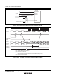
19.9.3 Note on Switchover of External Clock
When two or more external clocks (e.g. 16 MHz and 13 MHz) are used as the system clock,
switchover of the input clock should be carried out in software standby mode.
An example of an external clock switching circuit is shown in figure 19.11, and an example of the
external clock switchover timing in figure 19.12.