
Datasheet
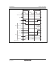
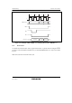
Table Of Contents
- Cover
- Notice
- General Precautions in the Handling of MPU/MCU Products
- Configuration of This Manual
- Preface
- Main Revisions for This Edition
- Contents
- Section 1 Overview
- Section 2 CPU
- 2.1 Features
- 2.2 CPU Operating Modes
- 2.3 Address Space
- 2.4 Register Configuration
- 2.5 Data Formats
- 2.6 Instruction Set
- 2.7 Addressing Modes and Effective Address Calculation
- 2.7.1 Register Direct—Rn
- 2.7.2 Register Indirect—@ERn
- 2.7.3 Register Indirect with Displacement—@(d:16, ERn) or @(d:32, ERn)
- 2.7.4 Register Indirect with Post-Increment or Pre-Decrement—@ERn+ or @-ERn
- 2.7.5 Absolute Address—@aa:8, @aa:16, @aa:24, or @aa:32
- 2.7.6 Immediate—#xx:8, #xx:16, or #xx:32
- 2.7.7 Program-Counter Relative—@(d:8, PC) or @(d:16, PC)
- 2.7.8 Memory Indirect—@@aa:8
- 2.7.9 Effective Address Calculation
- 2.8 Processing States
- 2.9 Usage Notes
- Section 3 MCU Operating Modes
- Section 4 Exception Handling
- Section 5 Interrupt Controller
- Section 6 Bus Controller
- Section 7 DMA Controller (DMAC)
- 7.1 Features
- 7.2 Register Configuration
- 7.3 Register Descriptions
- 7.4 Operation
- 7.4.1 Transfer Modes
- 7.4.2 Sequential Mode
- 7.4.3 Idle Mode
- 7.4.4 Repeat Mode
- 7.4.5 Normal Mode
- 7.4.6 Block Transfer Mode
- 7.4.7 DMAC Activation Sources
- 7.4.8 Basic DMAC Bus Cycles
- 7.4.9 DMAC Bus Cycles (Dual Address Mode)
- 7.4.10 DMAC Multi-Channel Operation
- 7.4.11 Relation between the DMAC, External Bus Requests, and the DTC
- 7.4.12 NMI Interrupts and DMAC
- 7.4.13 Forced Termination of DMAC Operation
- 7.4.14 Clearing Full Address Mode
- 7.5 Interrupts
- 7.6 Usage Notes
- Section 8 Data Transfer Controller (DTC)
- 8.1 Features
- 8.2 Register Descriptions
- 8.2.1 DTC Mode Register A (MRA)
- 8.2.2 DTC Mode Register B (MRB)
- 8.2.3 DTC Source Address Register (SAR)
- 8.2.4 DTC Destination Address Register (DAR)
- 8.2.5 DTC Transfer Count Register A (CRA)
- 8.2.6 DTC Transfer Count Register B (CRB)
- 8.2.7 DTC Enable Registers (DTCERA to DTCERF)
- 8.2.8 DTC Vector Register (DTVECR)
- 8.3 Activation Sources
- 8.4 Location of Register Information and DTC Vector Table
- 8.5 Operation
- 8.6 Procedures for Using DTC
- 8.7 Examples of Use of the DTC
- 8.8 Usage Notes
- Section 9 I/O Ports
- Section 10 16-Bit Timer Pulse Unit (TPU)
- 10.1 Features
- 10.2 Input/Output Pins
- 10.3 Register Descriptions
- 10.3.1 Timer Control Register (TCR)
- 10.3.2 Timer Mode Register (TMDR)
- 10.3.3 Timer I/O Control Register (TIOR)
- 10.3.4 Timer Interrupt Enable Register (TIER)
- 10.3.5 Timer Status Register (TSR)
- 10.3.6 Timer Counter (TCNT)
- 10.3.7 Timer General Register (TGR)
- 10.3.8 Timer Start Register (TSTR)
- 10.3.9 Timer Synchro Register (TSYR)
- 10.4 Interface to Bus Master
- 10.5 Operation
- 10.6 Interrupts
- 10.7 Operation Timing
- 10.8 Usage Notes
- Section 11 8-Bit Timers (TMR)
- 11.1 Features
- 11.2 Input/Output Pins
- 11.3 Register Descriptions
- 11.4 Operation
- 11.5 Operation Timing
- 11.6 Operation with Cascaded Connection
- 11.7 Interrupts
- 11.8 Usage Notes
- 11.8.1 Contention between TCNT Write and Clear
- 11.8.2 Contention between TCNT Write and Increment
- 11.8.3 Contention between TCOR Write and Compare Match
- 11.8.4 Contention between Compare Matches A and B
- 11.8.5 Switching of Internal Clocks and TCNT Operation
- 11.8.6 Mode Setting with Cascaded Connection
- 11.8.7 Module Stop Mode Setting
- Section 12 Watchdog Timer (WDT)
- Section 13 Serial Communication Interface
- 13.1 Features
- 13.2 Input/Output Pins
- 13.3 Register Descriptions
- 13.3.1 Receive Shift Register (RSR)
- 13.3.2 Receive Data Register (RDR)
- 13.3.3 Transmit Data Register (TDR)
- 13.3.4 Transmit Shift Register (TSR)
- 13.3.5 Serial Mode Register (SMR)
- 13.3.6 Serial Control Register (SCR)
- 13.3.7 Serial Status Register (SSR)
- 13.3.8 Smart Card Mode Register (SCMR)
- 13.3.9 Serial Extended Mode Register (SEMR) (Only for Channel 0 in H8S/2215)
- 13.3.10 Serial Extended Mode Register A_0 (SEMRA_0) (Only for Channel 0 in H8S/2215R, H8S/2215T and H8S/2215C)
- 13.3.11 Serial Extended Mode Register B_0 (SEMRB_0) (Only for Channel 0 in H8S/2215R, H8S/2215T and H8S/2215C)
- 13.3.12 Bit Rate Register (BRR)
- 13.4 Operation in Asynchronous Mode
- 13.5 Multiprocessor Communication Function
- 13.6 Operation in Clocked Synchronous Mode
- 13.7 Operation in Smart Card Interface
- 13.7.1 Pin Connection Example
- 13.7.2 Data Format (Except for Block Transfer Mode)
- 13.7.3 Clock
- 13.7.4 Block Transfer Mode
- 13.7.5 Receive Data Sampling Timing and Reception Margin
- 13.7.6 Initialization
- 13.7.7 Serial Data Transmission (Except for Block Transfer Mode)
- 13.7.8 Serial Data Reception (Except for Block Transfer Mode)
- 13.7.9 Clock Output Control
- 13.8 SCI Select Function
- 13.9 Interrupts
- 13.10 Usage Notes
- 13.10.1 Break Detection and Processing (Asynchronous Mode Only)
- 13.10.2 Mark State and Break Detection (Asynchronous Mode Only)
- 13.10.3 Receive Error Flags and Transmit Operations (Clocked Synchronous Mode Only)
- 13.10.4 Restrictions on Use of DMAC or DTC
- 13.10.5 Operation in Case of Mode Transition
- 13.10.6 Switching from SCK Pin Function to Port Pin Function
- 13.10.7 Module Stop Mode Setting
- Section 14 Boundary Scan Function
- Section 15 Universal Serial Bus Interface (USB)
- 15.1 Features
- 15.2 Input/Output Pins
- 15.3 Register Descriptions
- 15.3.1 USB Endpoint Information Registers 00_0 to 22_4 (UEPIR00_0 to UEPIR22_4)
- 15.3.2 USB Control Register (UCTLR)
- 15.3.3 USB DMAC Transfer Request Register (UDMAR)
- 15.3.4 USB Device Resume Register (UDRR)
- 15.3.5 USB Trigger Register 0 (UTRG0)
- 15.3.6 USB Trigger Register 1 (UTRG1)
- 15.3.7 USBFIFO Clear Register 0 (UFCLR0)
- 15.3.8 USBFIFO Clear Register 1 (UFCLR1)
- 15.3.9 USB Endpoint Stall Register 0 (UESTL0)
- 15.3.10 USB Endpoint Stall Register 1 (UESTL1)
- 15.3.11 USB Endpoint Data Register 0s (UEDR0s)
- 15.3.12 USB Endpoint Data Register 0i (UEDR0i)
- 15.3.13 USB Endpoint Data Register 0o (UEDR0o)
- 15.3.14 USB Endpoint Data Register 1i (UEDR1i)
- 15.3.15 USB Endpoint Data Register 2i (UEDR2i)
- 15.3.16 USB Endpoint Data Register 2o (UEDR2o)
- 15.3.17 USB Endpoint Data Register 3i (UEDR3i)
- 15.3.18 USB Endpoint Data Register 3o (UEDR3o)
- 15.3.19 USB Endpoint Data Register 4i (UEDR4i)
- 15.3.20 USB Endpoint Data Register 4o (UEDR4o)
- 15.3.21 USB Endpoint Data Register 5i (UEDR5i)
- 15.3.22 USB Endpoint Receive Data Size Register 0o (UESZ0o)
- 15.3.23 USB Endpoint Receive Data Size Register 2o (UESZ2o)
- 15.3.24 USB Endpoint Receive Data Size Register 3o (UESZ3o)
- 15.3.25 USB Endpoint Receive Data Size Register 4o (UESZ4o)
- 15.3.26 USB Interrupt Flag Register 0 (UIFR0)
- 15.3.27 USB Interrupt Flag Register 1 (UIFR1) (Only in H8S/2215)
- 15.3.28 USB Interrupt Flag Register 1 (UIFR1) (Only in H8S/2215R, H8S/2215T and H8S/2215C)
- 15.3.29 USB Interrupt Flag Register 2 (UIFR2) (Only in H8S/2215)
- 15.3.30 USB Interrupt Flag Register 2 (UIFR2) (Only in H8S/2215R, H8S/2215T and H8S/2215C)
- 15.3.31 USB Interrupt Flag Register 3 (UIFR3)
- 15.3.32 USB Interrupt Enable Register 0 (UIER0)
- 15.3.33 USB Interrupt Enable Register 1 (UIER1) (Only in H8S/2215)
- 15.3.34 USB Interrupt Enable Register 1 (UIER1) (Only in H8S/2215R, H8S/2215T and H8S/2215C)
- 15.3.35 USB Interrupt Enable Register 2 (UIER2)
- 15.3.36 USB Interrupt Enable Register 2 (UIER2) (Only in H8S/2215R, H8S/2215T and H8S/2215C)
- 15.3.37 USB Interrupt Enable Register 3 (UIER3)
- 15.3.38 USB Interrupt Select Register 0 (UISR0)
- 15.3.39 USB Interrupt Select Register 1 (UISR1) (Only in H8S/2215)
- 15.3.40 USB Interrupt Select Register 1 (UISR1) (Only in H8S/2215R, H8S/2215T and H8S/2215C)
- 15.3.41 USB Interrupt Select Register 2 (UISR2) (Only in H8S/2215)
- 15.3.42 USB Interrupt Select Register 2 (UISR2) (Only in H8S/2215R, H8S/2215T and H8S/2215C)
- 15.3.43 USB Interrupt Select Register 3 (UISR3)
- 15.3.44 USB Data Status Register (UDSR)
- 15.3.45 USB Configuration Value Register (UCVR)
- 15.3.46 USB Time Stamp Registers H, L (UTSRH, UTSRL)
- 15.3.47 USB Test Register 0 (UTSTR0)
- 15.3.48 USB Test Register 1 (UTSTR1)
- 15.3.49 USB Test Registers 2 and A to F (UTSTR2, UTSRA to UTSRF)
- 15.3.50 Module Stop Control Register B (MSTPCRB)
- 15.4 Interrupt Sources
- 15.5 Communication Operation
- 15.5.1 Initialization
- 15.5.2 USB Cable Connection/Disconnection
- 15.5.3 Suspend and Resume Operations
- 15.5.4 Control Transfer
- 15.5.5 Interrupt-In Transfer (EP1i Is specified as Endpoint)
- 15.5.6 Bulk-In Transfer (Dual FIFOs) (EP2i Is specified as Endpoint)
- 15.5.7 Bulk-Out Transfer (Dual FIFOs) (EP2o Is specified as Endpoint)
- 15.5.8 Isochronous—In Transfer (Dual-FIFO) (When EP3i Is Specified as Endpoint)
- 15.5.9 Isochronous—Out Transfer (Dual-FIFO) (When EP3o Is Specified as Endpoint)
- 15.5.10 Processing of USB Standard Commands and Class/Vendor Commands
- 15.5.11 Stall Operations
- 15.6 DMA Transfer Specifications
- 15.7 Endpoint Configuration Example
- 15.8 USB External Circuit Example
- 15.9 Usage Notes
- 15.9.1 Operating Frequency
- 15.9.2 Bus Interface
- 15.9.3 Setup Data Reception
- 15.9.4 FIFO Clear
- 15.9.5 IRQ6 Interrupt
- 15.9.6 Data Register Overread or Overwrite
- 15.9.7 EP3o Isochronous Transfer
- 15.9.8 Reset
- 15.9.9 EP0 Interrupt Assignment
- 15.9.10 Level Shifter for VBUS and IRQx Pins
- 15.9.11 Read and Write to USB Endpoint Data Register
- 15.9.12 Restrictions for Software Standby Mode Transition
- 15.9.13 USB External Circuit Example
- 15.9.14 Pin Processing when USB Not Used
- 15.9.15 Notes on Emulator Usage
- 15.9.16 Notes on TR Interrupt
- 15.9.17 Notes on UIFRO
- 15.9.18 Clearing the FIFOs in DMA Transfer Mode
- Section 16 A/D Converter
- Section 17 D/A Converter
- Section 18 RAM
- Section 19 Flash Memory (F-ZTAT Version)
- 19.1 Features
- 19.2 Mode Transitions
- 19.3 Block Configuration
- 19.4 Input/Output Pins
- 19.5 Register Descriptions
- 19.6 On-Board Programming Modes
- 19.7 Flash Memory Emulation in RAM
- 19.8 Flash Memory Programming/Erasing
- 19.9 Program/Erase Protection
- 19.10 Interrupt Handling when Programming/Erasing Flash Memory
- 19.11 Programmer Mode
- 19.12 Power-Down States for Flash Memory
- 19.13 Flash Memory Programming and Erasing Precautions
- 19.14 Note on Switching from F-ZTAT Version to Masked ROM Version
- Section 20 Masked ROM
- Section 21 Clock Pulse Generator
- Section 22 Power-Down Modes
- Section 23 List of Registers
- Section 24 Electrical Characteristics (H8S/2215)
- Section 25 Electrical Characteristics (H8S/2215R)
- Section 26 Electrical Characteristics (H8S/2215T)
- Section 27 Electrical Characteristics (H8S/2215C)
- Appendix
- Index
- Colophon
- Address List
- Back Cover
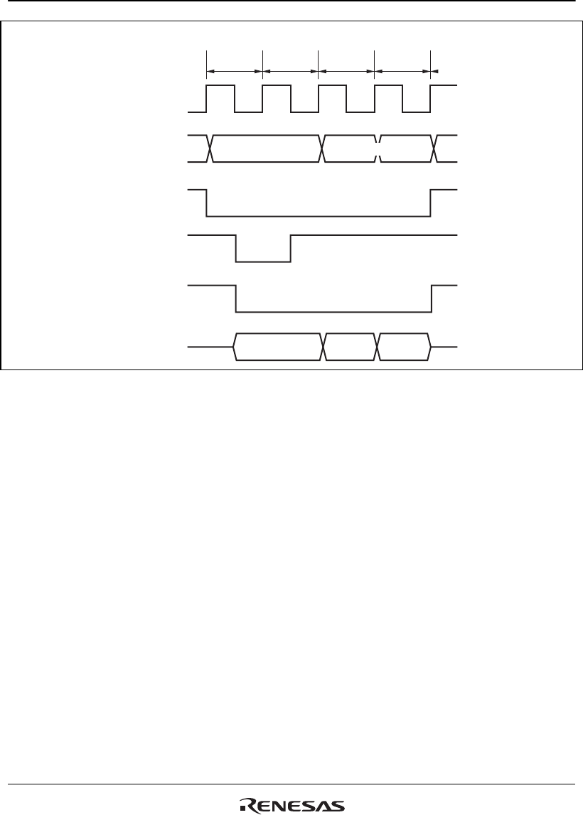
Section 6 Bus Controller
REJ09B0140-0900 Rev. 9.00 Page 141 of 846
Sep 16, 2010
H8S/2215 Group
T
1
CS0
AS
T
2
T
1
T
1
RD
Address bus
φ
Data bus
Full access Burst access
Only lower address changed
Read data Read data Read data
Figure 6.21 Example of Burst ROM Access Timing (When AST0 = BRSTS1 = 0)
6.7.2 Wait Control
As with the basic bus interface, either program wait insertion or pin wait insertion using the WAIT
pin can be used in the initial cycle (full access) of the burst ROM interface. See section 6.6.4, Wait
Control.
Wait states cannot be inserted in a burst cycle.