
Datasheet
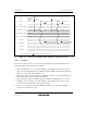
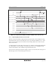
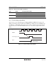
Table Of Contents
- Cover
- Notice
- General Precautions in the Handling of MPU/MCU Products
- Configuration of This Manual
- Preface
- Main Revisions for This Edition
- Contents
- Section 1 Overview
- Section 2 CPU
- 2.1 Features
- 2.2 CPU Operating Modes
- 2.3 Address Space
- 2.4 Register Configuration
- 2.5 Data Formats
- 2.6 Instruction Set
- 2.7 Addressing Modes and Effective Address Calculation
- 2.7.1 Register Direct—Rn
- 2.7.2 Register Indirect—@ERn
- 2.7.3 Register Indirect with Displacement—@(d:16, ERn) or @(d:32, ERn)
- 2.7.4 Register Indirect with Post-Increment or Pre-Decrement—@ERn+ or @-ERn
- 2.7.5 Absolute Address—@aa:8, @aa:16, @aa:24, or @aa:32
- 2.7.6 Immediate—#xx:8, #xx:16, or #xx:32
- 2.7.7 Program-Counter Relative—@(d:8, PC) or @(d:16, PC)
- 2.7.8 Memory Indirect—@@aa:8
- 2.7.9 Effective Address Calculation
- 2.8 Processing States
- 2.9 Usage Notes
- Section 3 MCU Operating Modes
- Section 4 Exception Handling
- Section 5 Interrupt Controller
- Section 6 Bus Controller
- Section 7 DMA Controller (DMAC)
- 7.1 Features
- 7.2 Register Configuration
- 7.3 Register Descriptions
- 7.4 Operation
- 7.4.1 Transfer Modes
- 7.4.2 Sequential Mode
- 7.4.3 Idle Mode
- 7.4.4 Repeat Mode
- 7.4.5 Normal Mode
- 7.4.6 Block Transfer Mode
- 7.4.7 DMAC Activation Sources
- 7.4.8 Basic DMAC Bus Cycles
- 7.4.9 DMAC Bus Cycles (Dual Address Mode)
- 7.4.10 DMAC Multi-Channel Operation
- 7.4.11 Relation between the DMAC, External Bus Requests, and the DTC
- 7.4.12 NMI Interrupts and DMAC
- 7.4.13 Forced Termination of DMAC Operation
- 7.4.14 Clearing Full Address Mode
- 7.5 Interrupts
- 7.6 Usage Notes
- Section 8 Data Transfer Controller (DTC)
- 8.1 Features
- 8.2 Register Descriptions
- 8.2.1 DTC Mode Register A (MRA)
- 8.2.2 DTC Mode Register B (MRB)
- 8.2.3 DTC Source Address Register (SAR)
- 8.2.4 DTC Destination Address Register (DAR)
- 8.2.5 DTC Transfer Count Register A (CRA)
- 8.2.6 DTC Transfer Count Register B (CRB)
- 8.2.7 DTC Enable Registers (DTCERA to DTCERF)
- 8.2.8 DTC Vector Register (DTVECR)
- 8.3 Activation Sources
- 8.4 Location of Register Information and DTC Vector Table
- 8.5 Operation
- 8.6 Procedures for Using DTC
- 8.7 Examples of Use of the DTC
- 8.8 Usage Notes
- Section 9 I/O Ports
- Section 10 16-Bit Timer Pulse Unit (TPU)
- 10.1 Features
- 10.2 Input/Output Pins
- 10.3 Register Descriptions
- 10.3.1 Timer Control Register (TCR)
- 10.3.2 Timer Mode Register (TMDR)
- 10.3.3 Timer I/O Control Register (TIOR)
- 10.3.4 Timer Interrupt Enable Register (TIER)
- 10.3.5 Timer Status Register (TSR)
- 10.3.6 Timer Counter (TCNT)
- 10.3.7 Timer General Register (TGR)
- 10.3.8 Timer Start Register (TSTR)
- 10.3.9 Timer Synchro Register (TSYR)
- 10.4 Interface to Bus Master
- 10.5 Operation
- 10.6 Interrupts
- 10.7 Operation Timing
- 10.8 Usage Notes
- Section 11 8-Bit Timers (TMR)
- 11.1 Features
- 11.2 Input/Output Pins
- 11.3 Register Descriptions
- 11.4 Operation
- 11.5 Operation Timing
- 11.6 Operation with Cascaded Connection
- 11.7 Interrupts
- 11.8 Usage Notes
- 11.8.1 Contention between TCNT Write and Clear
- 11.8.2 Contention between TCNT Write and Increment
- 11.8.3 Contention between TCOR Write and Compare Match
- 11.8.4 Contention between Compare Matches A and B
- 11.8.5 Switching of Internal Clocks and TCNT Operation
- 11.8.6 Mode Setting with Cascaded Connection
- 11.8.7 Module Stop Mode Setting
- Section 12 Watchdog Timer (WDT)
- Section 13 Serial Communication Interface
- 13.1 Features
- 13.2 Input/Output Pins
- 13.3 Register Descriptions
- 13.3.1 Receive Shift Register (RSR)
- 13.3.2 Receive Data Register (RDR)
- 13.3.3 Transmit Data Register (TDR)
- 13.3.4 Transmit Shift Register (TSR)
- 13.3.5 Serial Mode Register (SMR)
- 13.3.6 Serial Control Register (SCR)
- 13.3.7 Serial Status Register (SSR)
- 13.3.8 Smart Card Mode Register (SCMR)
- 13.3.9 Serial Extended Mode Register (SEMR) (Only for Channel 0 in H8S/2215)
- 13.3.10 Serial Extended Mode Register A_0 (SEMRA_0) (Only for Channel 0 in H8S/2215R, H8S/2215T and H8S/2215C)
- 13.3.11 Serial Extended Mode Register B_0 (SEMRB_0) (Only for Channel 0 in H8S/2215R, H8S/2215T and H8S/2215C)
- 13.3.12 Bit Rate Register (BRR)
- 13.4 Operation in Asynchronous Mode
- 13.5 Multiprocessor Communication Function
- 13.6 Operation in Clocked Synchronous Mode
- 13.7 Operation in Smart Card Interface
- 13.7.1 Pin Connection Example
- 13.7.2 Data Format (Except for Block Transfer Mode)
- 13.7.3 Clock
- 13.7.4 Block Transfer Mode
- 13.7.5 Receive Data Sampling Timing and Reception Margin
- 13.7.6 Initialization
- 13.7.7 Serial Data Transmission (Except for Block Transfer Mode)
- 13.7.8 Serial Data Reception (Except for Block Transfer Mode)
- 13.7.9 Clock Output Control
- 13.8 SCI Select Function
- 13.9 Interrupts
- 13.10 Usage Notes
- 13.10.1 Break Detection and Processing (Asynchronous Mode Only)
- 13.10.2 Mark State and Break Detection (Asynchronous Mode Only)
- 13.10.3 Receive Error Flags and Transmit Operations (Clocked Synchronous Mode Only)
- 13.10.4 Restrictions on Use of DMAC or DTC
- 13.10.5 Operation in Case of Mode Transition
- 13.10.6 Switching from SCK Pin Function to Port Pin Function
- 13.10.7 Module Stop Mode Setting
- Section 14 Boundary Scan Function
- Section 15 Universal Serial Bus Interface (USB)
- 15.1 Features
- 15.2 Input/Output Pins
- 15.3 Register Descriptions
- 15.3.1 USB Endpoint Information Registers 00_0 to 22_4 (UEPIR00_0 to UEPIR22_4)
- 15.3.2 USB Control Register (UCTLR)
- 15.3.3 USB DMAC Transfer Request Register (UDMAR)
- 15.3.4 USB Device Resume Register (UDRR)
- 15.3.5 USB Trigger Register 0 (UTRG0)
- 15.3.6 USB Trigger Register 1 (UTRG1)
- 15.3.7 USBFIFO Clear Register 0 (UFCLR0)
- 15.3.8 USBFIFO Clear Register 1 (UFCLR1)
- 15.3.9 USB Endpoint Stall Register 0 (UESTL0)
- 15.3.10 USB Endpoint Stall Register 1 (UESTL1)
- 15.3.11 USB Endpoint Data Register 0s (UEDR0s)
- 15.3.12 USB Endpoint Data Register 0i (UEDR0i)
- 15.3.13 USB Endpoint Data Register 0o (UEDR0o)
- 15.3.14 USB Endpoint Data Register 1i (UEDR1i)
- 15.3.15 USB Endpoint Data Register 2i (UEDR2i)
- 15.3.16 USB Endpoint Data Register 2o (UEDR2o)
- 15.3.17 USB Endpoint Data Register 3i (UEDR3i)
- 15.3.18 USB Endpoint Data Register 3o (UEDR3o)
- 15.3.19 USB Endpoint Data Register 4i (UEDR4i)
- 15.3.20 USB Endpoint Data Register 4o (UEDR4o)
- 15.3.21 USB Endpoint Data Register 5i (UEDR5i)
- 15.3.22 USB Endpoint Receive Data Size Register 0o (UESZ0o)
- 15.3.23 USB Endpoint Receive Data Size Register 2o (UESZ2o)
- 15.3.24 USB Endpoint Receive Data Size Register 3o (UESZ3o)
- 15.3.25 USB Endpoint Receive Data Size Register 4o (UESZ4o)
- 15.3.26 USB Interrupt Flag Register 0 (UIFR0)
- 15.3.27 USB Interrupt Flag Register 1 (UIFR1) (Only in H8S/2215)
- 15.3.28 USB Interrupt Flag Register 1 (UIFR1) (Only in H8S/2215R, H8S/2215T and H8S/2215C)
- 15.3.29 USB Interrupt Flag Register 2 (UIFR2) (Only in H8S/2215)
- 15.3.30 USB Interrupt Flag Register 2 (UIFR2) (Only in H8S/2215R, H8S/2215T and H8S/2215C)
- 15.3.31 USB Interrupt Flag Register 3 (UIFR3)
- 15.3.32 USB Interrupt Enable Register 0 (UIER0)
- 15.3.33 USB Interrupt Enable Register 1 (UIER1) (Only in H8S/2215)
- 15.3.34 USB Interrupt Enable Register 1 (UIER1) (Only in H8S/2215R, H8S/2215T and H8S/2215C)
- 15.3.35 USB Interrupt Enable Register 2 (UIER2)
- 15.3.36 USB Interrupt Enable Register 2 (UIER2) (Only in H8S/2215R, H8S/2215T and H8S/2215C)
- 15.3.37 USB Interrupt Enable Register 3 (UIER3)
- 15.3.38 USB Interrupt Select Register 0 (UISR0)
- 15.3.39 USB Interrupt Select Register 1 (UISR1) (Only in H8S/2215)
- 15.3.40 USB Interrupt Select Register 1 (UISR1) (Only in H8S/2215R, H8S/2215T and H8S/2215C)
- 15.3.41 USB Interrupt Select Register 2 (UISR2) (Only in H8S/2215)
- 15.3.42 USB Interrupt Select Register 2 (UISR2) (Only in H8S/2215R, H8S/2215T and H8S/2215C)
- 15.3.43 USB Interrupt Select Register 3 (UISR3)
- 15.3.44 USB Data Status Register (UDSR)
- 15.3.45 USB Configuration Value Register (UCVR)
- 15.3.46 USB Time Stamp Registers H, L (UTSRH, UTSRL)
- 15.3.47 USB Test Register 0 (UTSTR0)
- 15.3.48 USB Test Register 1 (UTSTR1)
- 15.3.49 USB Test Registers 2 and A to F (UTSTR2, UTSRA to UTSRF)
- 15.3.50 Module Stop Control Register B (MSTPCRB)
- 15.4 Interrupt Sources
- 15.5 Communication Operation
- 15.5.1 Initialization
- 15.5.2 USB Cable Connection/Disconnection
- 15.5.3 Suspend and Resume Operations
- 15.5.4 Control Transfer
- 15.5.5 Interrupt-In Transfer (EP1i Is specified as Endpoint)
- 15.5.6 Bulk-In Transfer (Dual FIFOs) (EP2i Is specified as Endpoint)
- 15.5.7 Bulk-Out Transfer (Dual FIFOs) (EP2o Is specified as Endpoint)
- 15.5.8 Isochronous—In Transfer (Dual-FIFO) (When EP3i Is Specified as Endpoint)
- 15.5.9 Isochronous—Out Transfer (Dual-FIFO) (When EP3o Is Specified as Endpoint)
- 15.5.10 Processing of USB Standard Commands and Class/Vendor Commands
- 15.5.11 Stall Operations
- 15.6 DMA Transfer Specifications
- 15.7 Endpoint Configuration Example
- 15.8 USB External Circuit Example
- 15.9 Usage Notes
- 15.9.1 Operating Frequency
- 15.9.2 Bus Interface
- 15.9.3 Setup Data Reception
- 15.9.4 FIFO Clear
- 15.9.5 IRQ6 Interrupt
- 15.9.6 Data Register Overread or Overwrite
- 15.9.7 EP3o Isochronous Transfer
- 15.9.8 Reset
- 15.9.9 EP0 Interrupt Assignment
- 15.9.10 Level Shifter for VBUS and IRQx Pins
- 15.9.11 Read and Write to USB Endpoint Data Register
- 15.9.12 Restrictions for Software Standby Mode Transition
- 15.9.13 USB External Circuit Example
- 15.9.14 Pin Processing when USB Not Used
- 15.9.15 Notes on Emulator Usage
- 15.9.16 Notes on TR Interrupt
- 15.9.17 Notes on UIFRO
- 15.9.18 Clearing the FIFOs in DMA Transfer Mode
- Section 16 A/D Converter
- Section 17 D/A Converter
- Section 18 RAM
- Section 19 Flash Memory (F-ZTAT Version)
- 19.1 Features
- 19.2 Mode Transitions
- 19.3 Block Configuration
- 19.4 Input/Output Pins
- 19.5 Register Descriptions
- 19.6 On-Board Programming Modes
- 19.7 Flash Memory Emulation in RAM
- 19.8 Flash Memory Programming/Erasing
- 19.9 Program/Erase Protection
- 19.10 Interrupt Handling when Programming/Erasing Flash Memory
- 19.11 Programmer Mode
- 19.12 Power-Down States for Flash Memory
- 19.13 Flash Memory Programming and Erasing Precautions
- 19.14 Note on Switching from F-ZTAT Version to Masked ROM Version
- Section 20 Masked ROM
- Section 21 Clock Pulse Generator
- Section 22 Power-Down Modes
- Section 23 List of Registers
- Section 24 Electrical Characteristics (H8S/2215)
- Section 25 Electrical Characteristics (H8S/2215R)
- Section 26 Electrical Characteristics (H8S/2215T)
- Section 27 Electrical Characteristics (H8S/2215C)
- Appendix
- Index
- Colophon
- Address List
- Back Cover
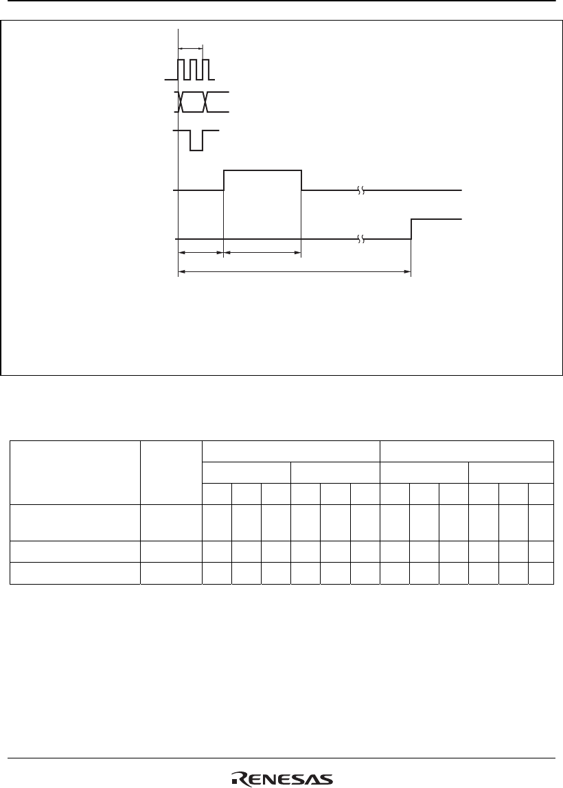
Section 16 A/D Converter
REJ09B0140-0900 Rev. 9.00 Page 611 of 846
Sep 16, 2010
H8S/2215 Group
(1)
(2)
t
D
t
SPL
t
CONV
φ
Address
Write signal
Input sampling
timing
ADF
Legend:
(1): ADCSR write cycle
(2): ADCSR address
t
D
: A/D conversion start delay
t
SPL
: Input sampling time
t
CONV
: A/D conversion time
Figure 16.5 A/D Conversion Timing
Table 16.3 A/D Conversion Time (Single Mode)
CKS1 = 0 CKS1 = 1
CKS0 = 0 CKS0 = 1 CKS0 = 0 CKS0 = 1
Item Symbol
Min Typ Max Min Typ Max Min Typ Max Min Typ Max
A/D conversion start
delay
t
D
18 — 33 10 — 17 6 — 9 4 — 5
Input sampling time t
SPL
— 127 — — 63 — — 31 — — 15 —
A/D conversion time t
CONV
515 — 530 259 — 266 131 — 134 67 — 68
Note: All values represent the number of states.