
Emulation Pod User's Manual


( 53 / 72 )
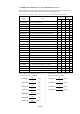
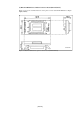
(4) Timing Requirements
Table 5.5, Figures 5.4 and 5.5 show timing requirements in the memory expansion mode and the
microprocessor mode.
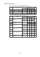
Table 5.5 Timing requirements (VCC=5V)
*1 Minimum 13ns (The definition is different from that of the actual MCU. For details, see Figure 5.5.)
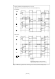
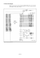
Figure 5.4 Timing requirements
Memory expansion mode and microprocessor mode
(only for "with wait")
BCLK
Conditions:
• V
CC=5V
• Input timing voltage: VIL=1.0V, VIH=4.0V
• Output timing voltage: VOL=2.5V, VOH=2.5V
Tsu (DB-RD)
Tsu (RDY-BCLK)
Tsu (HOLD-BCLK)
Th (RD-DB)
Th (BCLK-RDY)
Th (BCLK-HOLD)
Td (BCLK-HLDA)
Data input setup time
RDY* input setup time
HOLD* input setup time
Data input hold time
RDY* input hold time
HOLD* input hold time
HLDA* output delay time
Min.
40
30
40
0
0
0
Max.
40
Min.
50
(*1)
Max.
Actual MCU
[ns]
This product
[ns]
Symbol
Item
See left
See left
See left
See left
See left
RD
(separate bus)
WR, WRL, WRH
(separate bus)
RD
(multiplex bus)
WR, WRL, WRH
(multiplex bus)
RDY input