
Emulation Probe User's Manual

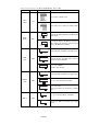
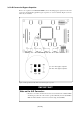
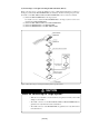
Table Of Contents
- Preface
- Contents
- 1. Precautions for Safety
- 2. Preparation
- 3. Setting Up
- 3.1 Selecting Clock Supply
- 3.2 Using an Internal Oscillator Circuit Board
- 3.3 Using the Oscillator Circuit on the Target System
- 3.4 Using the Internal Oscillator Circuit
- 3.5 Setting Switches
- 3.6 A-D Conversion Bypass Capacitor
- 3.7 Connecting the PC7501
- 3.8 Connecting the Target System
- (1) Connecting to a 100-pin LCC Socket
- (2) Connecting to a 100-pin 0.65-mm-pitch Foot Pattern (Part 1)
- (3) Connecting to a 100-pin 0.65-mm-pitch Foot Pattern (Part 2)
- (4) Connecting to a 100-pin 0.65-mm-pitch Foot Pattern (Part 3)
- (5) Connecting to a 100-pin 0.5-mm-pitch Foot Pattern (Part 1)
- (6) Connecting to a 100-pin 0.5-mm-pitch Foot Pattern (Part 2)
- (7) Connecting to a 100-pin 0.5-mm-pitch Foot Pattern (Part 3)
- (8) Connecting to a 144-pin 0.5-mm-pitch Foot Pattern
- 4. Usage
- 5. Specifications
- 6. Troubleshooting
- 7. Maintenance and Guarantee
( 35 / 76 )
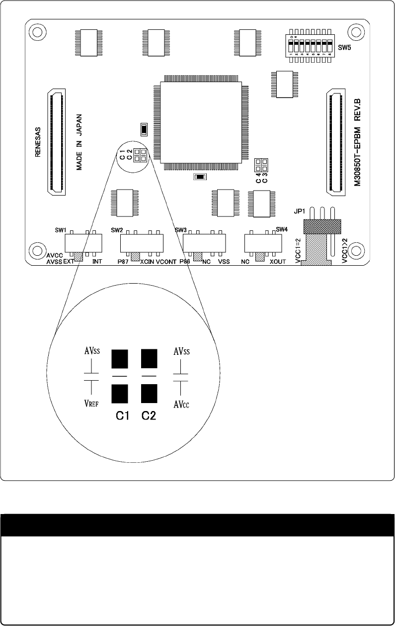
3.6 A-D Conversion Bypass Capacitor
There is a foot pattern on the M30850T-EPBM board for mounting bypass capacitors for the A-D
conversion circuit. Mount applicable bypass capacitors as occasion demands. Figure 3.8 shows
where they are installed.
IMPORTANT
Note on the A-D Converter:
• Because a converter board and other devices are used between the evaluation MCU
and the target system, the A-D converter operates differently from an actual MCU.
Make the final evaluation of the A-D converter using an actual MCU.
Figure 3.8 Foot pattern for the A-D conversion bypass capacitor
C1: VREF--AVSS bypass capacitor
C2: AVCC--AVSS bypass capacitor