October H8S and H8/300H 1 6 - B i t M i c r o c o n t r o l l e r s 2 1 - 0 1 8 F 1999
INDEX H8S and H8/300H Introduction 2 CPU 5 Instruction set Addressing Low power modes Exceptions and interrupts 6 7 8 9 1 6 - B i t M i c r o c o n t r o l l e r s Memory Peripherals Bus State Controller (BSC) Direct Memory Access Control (DMAC) Data Transfer Controller (DTC) Timer Timing Pattern Controller (TPC) and Programmable Pulse Generator (PPG) Serial Communication Interface (SCI) 10 12 14 15 16 20 21 Smart Card Interface 28 Analog to Digital Converter (ADC) and Digital to Analog Convert
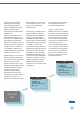
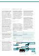
W e l c o m e T o Hitachi’s 16-bit microcontroller families customers, H8/300H is an excellent H8S and H8/300H. example where this policy has worked for our customers and Hitachi.
The European electronics industry produces and ships over 20 million H8 From a statistics point of view, every day demands full service and support. microcontrollers every month, in a vast 2 customers decide to use a 16-bit Hitachi, responded by setting up a range of advanced packaging and microcontroller made by Hitachi. European engineering and tool design temperature options.
H 8 S R o a d m a p Performance/ Memory/ Integration H8S+CAN (F)* H8S/2655 series up to 128K/4K Multiply-Accumulate H8S/2633 series (F)* up to 256K/16K Multiply-Accumulate H8S/267x series (F)* up to 256K/8K Multiply-Accumulate 20MHz at 5V 25MHz at 3.3V 33MHz at 3.3V H8S/2357 series (F) up to 128K/8K H8S/2345 series (F) up to 128K/4K H8S/232x series (F) up to 256K/8K 20MHz at 5V 20MHz at 5V 25MHz at 3.
C P U All H8 share a common CPU Being general purpose there is no In addition to the general purpose architecture, a general purpose register restriction placed on how each register is registers there are two control registers, a architecture that allows efficient used, thus they can be used for pointer Condition Code Register (CCR) and a execution of software written in C and or data operations. The architecture also Program Counter (PC). The CCR is an produces dense code.
I n s t r u c t i o n S e t H8/300H has an instruction set which Function Instruction suits the combined needs of HLL Data transfer MOV, PUSH, POP, MOVTPE, MOVFPE, LDM, STM programming and embedded applications. Arithmetic ADD, SUB, ADDX, SUBX, INC, DEC, ADDS, SUBS, It comprises of 62 instructions, with an operations DAA, DAS, MULXU, DIVXU, MULXS, DIVXS, CMP, emphasis on arithmetic instructions, NEG, EXTS, EXTU, TAS, MAC, LDMAC, STMAC, address manipulation and bit processing.
Pr ocessing A d d r e s s i n g In microcontroller applications it is often To support large memory systems, the available addressing modes. Supporting necessary to manipulate data on a bit by linear address space of the H8/300H and both, array and stack data types, the CPU bit basis. A good example would be the H8S CPU core allows direct access has indirect addressing with either where an I/O pin needs to be set to to every address in the whole 16MByte postincrement or predecrement.
L o w P o w e r In today’s electronics industry, low power consumption is an ever increasing concern for many engineers. Beyond Current dissipation (mA) Conditions: 15 HD6472246 typ. Sample 10Mhz/3.
required. Hence, very low average As an example for such a combination, power consumption can be achieved, let’s assume the DTC would be used to even with a real time clock being move results of ADC conversions from implemented in software. the ADC to a RAM buffer (e. g. 64 • If no activity is required, but RAM Byte). The CPU does not need to contents must be retained, H8/H8S process the data before acquisition of all microcontrollers can be brought into data has finished.
E x c e p t i o n s a n d I n t e r r u p t C o n t r o l l e r Trap instr uction exceptions (TRAPA) priority interrupt sources, which are capable of interrupting a low priority ISR which is already running. The These exceptions start when a TRAPA priority of individual interrupt sources instruction is executed in program is programmed in a number of execution state. The TRAPA instruction interrupt priority registers (IPR).
M e m o r y F L A S H consumption of Hitachi’s microcontrollers, • USER Mode such a redesign will often immediately User mode is not entered via reset. It eliminate radiation problems.
B u s S t a t e C o n t r o l l e r As one of the key reasons for using the ( B S C ) • DRAM access protocol for one area executes slow external write accesses H8S and H8/300H is the 16MBytes on 300H (=2Mbytes) and for 4 areas independently (on H8S/26xx and on linear address space, it will often be used on H8S (=8Mbytes)(not on all some H8S/23xx derivatives) and the in a system with a large amount of devices) improvement of read access time by external memory.
Impr oved access r ead timing state internal processing continues as long as there is no external access.The internal bus master, wishing to access the In order to give external devices a external bus during bus release state, may maximum of time to drive the required use the BREQO signal to indicate to the data onto the bus, the read access edge external master that the bus ownership that latches the data, has been moved to should be given back. The external bus the end of the cycle.
D i r e c t M e m o r y A c c e s s C o n t r o l l e r ( D M A C ) In a system with a high performance Some of the major improvements on performed between any area of the full CPU and with large memory, a Direct H8S are: 16MBytes address space. This mode Memory Access Controller will • A special transfer mode has been allows either a single transfer to occur significantly increase system performance.
D a t a T r a n s f e r C o n t r o l l e r ( D T C ) Analysis of many applications that use a the block, thus practically eliminating the takes 3 cycles and the actual data transfers DMAC has shown that a substantial part overhead penalty. take 2 cycles (minimum). maximum speed of data transfers. These Also, a single trigger can request multiple The DTC could be seen as a DMAC applications use a DMAC mainly to transfers (chain mode).
T i m e r One of the most important peripherals used. Hence, more money then is being the triggering of a DMA channel. on any microcontroller is the timer unit. spent on more powerful Channels 3 and 4 allow to produce a Timers have many uses in electronic microcontrollers, could be saved on pulse with duration down to one systems. They trigger the task switch of external devices, assembly cost, board clock cycle (62. 5ns at 16MHz).
• Timer Synchronisation To allow timer channels in the ITU The table below shows the PWM frequencies which can be obtained versus device clock speed and output resolution. possible to set up two or more timers PWM Res. 14-bit 16 MHz 976. 5 Hz 12 MHz 732. 7 Hz 10 MHz 610 Hz 8 MHz 488 Hz 6 MHz 365 Hz so that they are simultaneously 12-bit 3. 9 KHz 2. 9 KHz 2. 4 KHz 2 KHz 1. 5 KHz written to via software and cleared by 10-bit 15. 6 KHz 11. 7 KHz 9. 7 KHz 7. 8 KHz 5.
Modified H8/306x, and ITU on H8/3006 set the duty. reset However, as the ITU puts more emphasis on motor control and similar H8/3007 applications, the TPU does not support The ITU on H8/306x, H8/3006 and ‘Reset synchronized 6-phase PWM H8/3007 are modified to be more mode’ and ‘Complementary 6-phase flexible. Channels 3 and 4 can be split PWM mode’.
“mishap’ in the system (such as a noise seconds. This WDT can request an induced software crash) is rectified as interrupt, reset or NMI. If an interrupt quickly as possible. is requested this WDT is useful to update The principle behind a watchdog timer a software real time clock.
T i m i n g P a t t e r n C o n t r o l l e r ( T P C ) P r o g r a m m a b l e P u l s e G e n e r a t o r ( P P G ) These peripherals allow to generate Stepper Motor between new patterns being output to digital output signals in synchronisation Contr ol with allow acceleration and deceleration of the with a timer pulse, so that one could look TPC at them as ‘real time outputs’.
S e r i a l C o m m u n i c a t i o n s This form of communication has many uses in microcontroller applications, such I n t e r f a c e ( S C I ) H8/300H H8S H8S/21xx H8/3048 series Yes No as inter-device communications, Smart card interface (ISO 7816) diagnostics, host communication or as an Multi-processor mode Yes Yes Yes interface to peripherals. All of Hitachi’s IIC No H8S/2238 H8S/21x7, 8 SCI, even though most have two or IrDA No more.
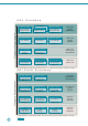
M e m o r y H H ROM-LESS or pseudo ROM-LESS(*) OTP and Mask (UD) Under Development 22 T y p e H H a n d S i z e Mask-ROM Flash and Mask (H8S/2623,33 Flash only)
H 8 S a n d H 8 / 3 0 0 H S e l e c t o r (UD) Under Development Vcc/Clock Memory Device H8/3001 H8/3002 H8/3003 H8/3004,5 H8/3006,7 H8/3020,1,2 (UD) ROM (byte) - - - - - 128,192,256k RAM (byte) 512 512 512 2,4k 2,4k 4,4,8k - - - - - HD64F3022 Vcc (V) / clock (MHz) 4.5-5.5/16 4.5-5.5/16 4.5-5.5/16 4.5-5.5/16 4.5-5.5/20 3.0-3.6/18 (During Operation) 3.0-5.5/13 3.0-5.5/10 3.0-5.5/10 4.5-5.5/18 3.0-5.5/13 2.7-5.5/8 2.7-5.5/8 2.7-5.5/8 3.0-5.5/10 2.7-5.
G u i d e H8/3030,1,2 H8/3033,4,5 H8/3036,7,8,9 H8/3040,1,2 H8/3044,5,7,8 H8/3052 (UD) H8/3060,1,2 H8/3065,6,7 H8S/2120,2,3,4,6,7,8** 16,32,64k 128,192,256k 16,32,64,128k 32,48,64k 32,64,98,128k 512k 64,96,128K 64,96,128K 32,64,128,96,32,64,128k 512,1k,2k 4k 512,1,2,4k 2k 2,2,4,4k 8k 2,4,4k 2,4,4k 2,2,4,4,2,2,4k HD6473032 HD6473035 HD64F3039 HD6473042 HD6473048 HD64F3052 HD64F3062 HD64F3067 HD64F2128 3.0-5.5/18 4.5-5.5/20 4.5-5.5/20 4.5-5.5/20 HD64F3048 4.5-5.
k H8S/2130,2,3,4,7,8** H8S/2142,3,4,7,8** H8S/2223,5,7 H8S/2233,5,7 H8S/2238 H8S/2240,1,2,3,4,5,6 H8S/2310,2 H8S/2322,3,7,8 H8S/2340,1,3,5 32,64,96,128,64,128k 64,96,128,64,128k 64,128,128k 64,128,128k 256k 0,32,32,64,64,128,128k - 0,32,128,256k 0,32,64,128k 2,2,4,4,2,4k 2,4,4,2,4k 4,4,16k 4,4,16k 16k 4,4,8,4,8,4,8k 2,8k 8k 2,2,2,4k HD64F2138 (128k) HD64F2148 (128k) HD6472237 HD6472237 HD64F2238 HD6472246 - HD64F2328 HD6472345 HD64F2134 (128k) HD64F2144 (128k) HD64F213
S/2350,1 Device H8S/2352,7 H8S/2623, H8S/2626 H8S/2633** H8S/2653,5 64,128k 0,128k 256k 256k 64,128k ROM (byte) 2k 2,4k 8k 12k 16k 4k RAM (byte) - HD6472355 HD6472357 HD64F2623 HD64F2633 HD6472655 OTP (HD647…) or FLASH (HD64F…) HD64F2357 HD64F2626 4.5-5.5/20 4.5-5.5/20 3.0-3.6/20 (Vcc) 3.0-3.6/25 (Vcc) 4.5-5.5/20 Vcc (V) / clock (MHz) 7-5.5/10 2.7-5.5/10 2.7-5.5/10* 4.5-5.5/20(PVcc) 4.5-5.5/25(PVcc) 2.7-5.5/10 (During Operation) Vcc=3.0-3.6 or 4.5-5.5 Vcc=3.0-3.
I n B r i e f In this brochure an overview is given as • Very powerful and sophisticated in the industry for many years to come. to why H8S and H8/300H give you the peripherals designed to reduce CPU The road map points towards: technical benefits that are demanded by overhead and hence to increase system • today’s applications.The purpose is to performance give you enough insight into the features • of the H8S and H8/300H family to see 33MHz at 3.
Smar t car d time normally used as stop bits, thus putting the smart card’s reset under inter face ISO7816-3 implements an error bit. host software control. mode That means, that a low level on the Also, a general purpose IO of the host is (SIM) RxD/TxD line at a particular position used to control a MOSFET that turns on In this mode the SCI conforms to a sub- after the data bits has to be recognised and off the power to the smart card. In set ISO7816-3.
A n a l o g u e t o D i g i t a l In many microcontroller based systems, High speed some way of measuring analogue H8S/2655 C o n v e r t e r ADC on electrical values is necessary. With this in ( A D C ) • Simultaneous sampling operation allows the two S&H to sample simultaneously. An important feature mind, all members of the H8S and On H8S/2655 Hitachi has implemented in some applications, e. g.
C o n t r o l l e r A r e a N e t w o r k C A N The HCAN module (Hitachi CAN)* likelihood of such a case increases in Hitachi’s HCAN module implements the complies to version 2.0B (Full CAN) as proportion to the length of the message. CAN standard by adding sophisticated defined by Bosch. Additionally, an Also, short messages keep latency low.
P37/D7 P36/D6 P35/D5 P34/D4 P33/D3 P32/D2 P31/D1 P30/D0 H 8 / 3 0 3 9 VCC VCC VSS VSS VSS Lowest cost H8/300H with Flash Port 3 Address bus Data bus (upper) MD2 MD1 MD0 EXTAL XTAL ø STBY RES RESO/FWE* NMI Port 5 Port 2 Port 8 Port 1 Serial communication interface (SCI) x 2 channels Programmable timing pattern controller (TPC) P17/A7 P16/A6 P15/A5 P14/A4 P13/A3 P12/A2 P11/A1 P10/A0 P95/SCK1/IRQ5 P94/SCK0/IRQ4 P93/RxD1 P92/RxD0 P91/TxD1 P90/TxD0 A/D converter Port A Port 7 PA7/TP7/TIOCB2/A20 P
VCC VCC VSS VSS VSS H 8 S / 2 1 3 4 NMI STBY P97/WAIT P96/ø/EXCL H8S/2000 CPU Interrupt controller P95/AS/IOS P94/HWR P27/A15 P26/A14 Port 2 MD1 MD0 Bus controller EXTAL Internal data bus Clock pulse generator RES XTAL Port 9 P93/RD P92/IRQ0 P91/IRQ1 P90/LWR/IRQ2/ADTRG P63/FTIB/CIN3/KIN3 P62/FTIA/CIN2/KIN2/TMIY RAM Port 6 P65/FTID/CIN5/KIN5 P64/FTIC/CIN4/KIN4 P13/A3 P12/A2 P11/A1 P10/A0 P37/D15 P36/D14 Port 3 14-bit PWM Port 4 P47/PWX1 P46/PWX0 P43/TMCI1 P42/TMRI0/SCK2 P15/A5 P14/A
Port A Port B PB7/ A15/TIOCB5 PB6/ A14/TIOCA5 PB5/ A13/TIOCB4 PB4/ A12/TIOCA4 PB3 / A11/TIOCD3 PB2/ A10/TIOCC3 PB1/ A9/TIOCB3 PB0/ A8/TIOCA3 Port C PC7/ A7 PC6/ A6 PC5/ A5 PC4/ A4 PC3/ A3 PC2/ A2 PC1/ A1 PC0/ A0 Port 3 P36 P35/ SCK1/IRQ5 P34/ RxD1 P33/ TxD1 P32/ SCK0/IRQ4 P31/ RxD0 P30/ TxD0 P97/ DA1 P96/DA0 Interrupt controller WDT1 (subclock operation) Port F SCI (4 channels) RAM D/A converter (2 channels) Port A 8-bit timer (4 channels) ROM Port F PF7 /ø PF6 / AS PF5 / RD PF4 / HWR PF3 / LWR
Port A Port B Port C ROM* PB7 /A15 PB6 /A14 PB5 /A13 PB4 /A12 PB3 / A11 PB2 /A10 PB1 /A9 PB0 /A8 PC7 /A7 PC6 /A6 PC5 /A5 PC4 /A4 PC3 /A3 PC2 /A2 PC1 /A1 PC0 /A0 Port 3 DTC PA3 / A19 PA2 / A18 PA1 / A17 PA0 / A16 P35 /SCK1/IRQ5 P34 /SCK0/IRQ4 P33 /RxD1 P32 /RxD0 P31 /TxD1 P30 /TxD0 Port 5 Peripheral data bus Interrupt controller Peripheral address bus H8S/2000 CPU Bus conbtroller PE7 /D7 PE6 /D6 PE5 /D5 PE4 /D4 PE3 /D3 PE2 /D2 PE1 /D1 PE0 /D0 Port E Interanal address bus Port D Internal data
Port F PG4 / CS0 PG3 / CS1 PG2 / CS2 PG1 / CS3 PG0 / CAS Port G Peripheral data bus PF7 /ø PF6 /AS PF5 /RD PF4 / HWR PF3 / LWR PF2 /LCAS/WAIT/BREQO PF1 / BACK PF0 / BREQ DTC DMAC ROM Port A PA7 / A23 / IRQ7 PA6 / A22 / IRQ6 PA5 / A21 / IRQ5 PA4 / A20 / IRQ4 PA3 / A19 PA2 / A18 PA1 / A17 PA0 / A16 Port B PB7 / A15 PB6 / A14 PB5 / A13 PB4 / A12 PB3 / A11 PB2 / A10 PB1 / A9 PB0 / A8 Port C PC7 / A7 PC6 / A6 PC5 / A5 PC4 / A4 PC3 / A3 PC2 / A2 PC1 / A1 PC0 / A0 Port 3 P35 / SCK1 P34 / SCK0 P33 /
PD7 / D15 PD6 / D14 PD5 / D13 PD4 / D12 PD3 / D11 PD2 / D10 PD1 / D9 PD0 / D8 PE7 /D7 PE6 /D6 PE5 /D5 PE4 /D4 PE3 /D3 PE2 /D2 PE1 /D1 PE0 /D0 PVCC1 PVCC2 VCC VCC VSS VSS VSS VSS VSS VSS H 8 S / 2 6 3 3 Port D Port E Port A Port B Port C Peripheral address bus SCI x 5 channels (IrDA x 1channel) I2C bus interface (option) 14-bit PWM timer TPU P37 /TxD4 P36 /RxD4 P35 /SCK1/SCK4/SCL0/IRQ5 P34 /RxD1/SDA0 P33 /TxD1/SCL1 P32 /SCK0/SDA1/IRQ4 P31 /RxD0/IrRxD P30 /TxD0/IrTxD P97 /AN15 P96 /AN14 P95 /AN13 P9
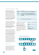
O r d e r i n g I n f o r m a t i o n The following tables show the available derivatives for each series within the H8/300H and H8S families.To build the actual part name append the desired clock rate to the part name’s body. Example: HD6413001F16 = H8/3001 in FP-80A package, 5V (±10%), 16MHz. For details (tolerance) of the operating voltage range, please refer to the selector guide in the middle of this brochure.
H 8 S O r d e r i n g I n f o r m a t i o n H8S/2128 (Flash) H8/3048 (OTP) Body Package suffix Package/Voltage/Temp. available clock Body Package suffix Package/Voltage HD6473048S F TF VF VTF FI TFI VFI VTFI FJ FP-100B/5V TFP-100B/5V FP-100B/low TFP-100B/low FP-100B/5V/-40°C..85°C TFP-100B/5V/-40°C..85°C FP-100B/low/-40°C..85°C TFP-100B/low/-40°C..85°C FP-100B/5V/-40°C..
H8S/2242 (pseudo ROM-less version) Body Vcc/clock suffix Package suffix HD6432242 A,M,K H8S/2355 (OTP) Package/Temp. 00FA FP-100B 00TE TFP-100B 00FAI FP-100B/-40°C..85°C 00TEI TFP-100B/-40°C..85°C Vcc/clock suffix: A=5V/20MHz, M=low/13MHz, K=low/10MHz Body Package/clock suffix Package/Voltage/Temp. HD6472355 F20 TE20 F10 TE10 F20I TE20I F10I TE10I FP-128/5V TFP-120/5V FP-128/low TFP-120/low FP-128/5V/-40°C..85°C TFP-120/5V/-40°C..85°C FP-128/low/-40°C..85°C TFP-120/low/-40°C..
O r d e r i n g Naming r ule H8/300H I n f o r m a t i o n for mask ROM a n d P a c k a g e s x 14mm) in standard spec. xx will be standard ROM-less commercial criteria determined after ROM code submission. apply (e. g. minimum order quantity). par ts The part names comply with the Naming HD643 + device body+ revision + H8S r ule mask for ROM par ts masked ROM naming rule (please see above).
P a c k a g e s Unit: mm 24.8 ± 0.4 Unit: mm 22.0 ± 0.2 20 20 80 51 65 0.20 +0.10 –0.20 0.15 0.5 0.75 0° – 10° 1.2 ± 0.2 0.10 Dimension including the plating thickness Base material dimension 0.17 ± 0.05 0.15 ± 0.04 2.70 0.10 M 3.15 Max 0.22 ± 0.05 0.20 ± 0.04 2.4 0.83 +0.15 –0.10 0.58 39 38 1.0 0.75 0° – 10° 0.5 ± 0.2 0.10 2.70 M 0.17 ± 0.05 0.15 ± 0.04 0.13 128 1 30 3.10 Max 1 0.32 ± 0.08 0.30 ± 0.06 14 31 16.0 ± 0.2 100 64 103 0.65 50 14 18.8 ± 0.
P a c k a g e s Unit: mm 16.0 ± 0.2 14 90 61 60 0.4 16.0 ± 0.2 91 120 0.10 0.17 ± 0.05 0.15 ± 0.04 1.00 0.07 M 1.2 1.20 Max 31 30 0.10 ± 0.10 1 0.17 ± 0.05 0.15 ± 0.04 1.0 0° – 8° 0.5 ± 0.
T o o l s * Emulators Hitachi provides fully-featured incircuit, real-time emulators for all of its devices, at a very competitive price/performance ratio. The first-generation H8/300H devices are supported by PCE’s (PC based emulators).
C-Compiler/Hitachi spent on learning how to operate the Workbench tool is short, errors in usage are reduced and the project is kept under tight Hitachi’s C-Compiler is designed to control.
HDI Debugger MakeApp FLASH pr ogramming softwar e (FDT) HDI is Hitachi’s debugging interface MakeApp is a visual development tool, used for all development tools ranging which automatically creates device dri- Hitachi provides free Windows software from evaluation boards to emulators. vers for all the on-chip peripherals. It which conveniently supports This enables engineers to move provides a point and click mechanism to programming its Flash microcontrollers.
T h i r d T o o l s P a r t y Thir d Par ty Operating Thir d Systems Par ty Emulators Third party operating systems that support H8/300H and H8S are available H8/300H and H8S are being supported from ATI and TECSI. Both companies by several renowned third party emulator offer modern real time operating systems manufacturers.
Related Literatur e Inter net / / Hitachi CD-ROM CD-ROM ‘Hitachi Electr onic Components Shortforms for Hitachi Databook Microcontroller Literature no. ‘H8/300 & H8/300L’ 21-017 16-008 This CD-ROM is available free of charge from Hitachi or our authorized Hitachi’s single chip, low power H8 family distributors.
The application notes listed are available for Hitachi’s 16-bit microcontrollers. You will find them on our CD-ROM as well as on Hitachi’s web-site (address URL: http://www. hitachi-eu. com/hel/ecg/index. htm). Please note that most of these application notes are easily modified to be used on H8S. Application Notes No. DMA request and Transfer time on H8/300H Apps/012/1.0 Interfacing various bit-size DRAMS to the H8/300H Apps/013/1.0 Add. the damping resistor to the osc.
http://www.hitachi-eu.com/hel/ecg/ Hitachi Europe Ltd Hitachi Europe GmbH Electronic Components Group Electronics Components Group Nissei Sangyo GmbH* (Northern Europe) Continental Europe Headquarters: Sales Offices: Dorncher Str. 3, D-85622 Feldkirchen Whitebrook Park, Lower Cookham Road, Germany Tel: Maidenhead, Berkshire SL6 8YA UK Dornacher Str.