REG10J0131-0100 Renesas Starter Kit for H8SX/1668R User’s Manual RENESAS SINGLE-CHIP MICROCOMPUTER H8SX FAMILY Rev.1.00 Revision date: 04.APR.2008 Renesas Technology Europe Ltd. www.renesas.
Table of Contents Chapter 1. Preface ....................................................................................................................................................................................... 3 Chapter 2. Purpose ...................................................................................................................................................................................... 4 Chapter 3. Power Supply..............................................................
Chapter 1. Preface Cautions This document may be, wholly or partially, subject to change without notice. All rights reserved. Duplication of this document, either in whole or part is prohibited without the written permission of Renesas Technology Europe Limited. Trademarks All brand or product names used in this manual are trademarks or registered trademarks of their respective companies or organisations. Copyright © Renesas Technology Europe Ltd. 2008. All rights reserved. © Renesas Technology Corporation.
Chapter 2. Purpose This RSK is an evaluation tool for Renesas microcontrollers. This manual describes the technical details of the RSK hardware. The Quick Start Guide and Tutorial Manual provide details of the software installation and debugging environment. Features include: • Renesas Microcontroller Programming. • User Code Debugging. • User Circuitry such as Switches, LEDs and potentiometer. • User or Example Application. • Sample peripheral device initialisation code.
Chapter 3. Power Supply 3.1. Requirements This RSK operates from a 5V power supply. A diode provides reverse polarity protection only if a current limiting power supply is used. All RSK boards are supplied with an E10A debugger. All RSK boards have an optional centre positive supply connector using a 2.0mm barrel power jack. Warning The RSK is neither under nor over voltage protected. Use a centre positive supply for this board. 3.2.
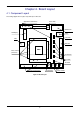
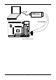
Chapter 4. Board Layout 4.1. Component Layout The following diagram shows top layer component layout of the board.
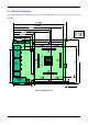
4.2. Board Dimensions The following diagram gives the board dimensions and connector positions. All through hole connectors are on a common 0.1” grid for easy 14.00mm 3.81mm Figure 4-2: Board Dimensions 7 100.00mm 85.00mm RING Applies to connector with micriocontroller pin1 Application Header JA3 5.00mm 80.01mm interfacing.
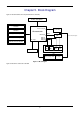
Chapter 5. Block Diagram Figure 5-1 shows the CPU board components and their connectivity.
E8 E10A Figure 5-2: RSK Connections 9
Chapter 6. User Circuitry 6.1. Switches There are four switches located on the CPU board. The function of each switch and its connection are shown in Table 6-1. Switch Function Microcontroller RES When pressed, the RSK microcontroller is reset. RESn, Pin 91 SW1/BOOT* Connects to an IRQ input for user controls. IRQ0n, Pin 84 The switch is also used in conjunction with the RES switch to place the device in (Port 1 pin 0) BOOT mode when not using the E10A debugger.
Description Function Circuit Net CPU’s Name Pin Fit for RS232 Remove for RS232 SCI0 Default serial port TXD0 52 R31 R37 SCI0 Default serial port RXD0 51 R30 R36 SCI5 Spare Serial Port TXD5 93 R34, R15 - SCI5 Spare Serial Port RXD5 94 R35, R28 - Table 6-3: Serial Port settings The SCI0 port is also available on J2 and JA2 (R59 and R70 must be fitted) headers. The SCI5 port is available on J3 and JA6 headers.. 6.5.
Option Link Settings Reference R15 R19 R28 R30 R31 R32 R33 R34 R35 R36 Function Fitted Alternative (Removed) Related To Serial Port Connects serial port SCI5 (Tx) to Disconnects serial port SCI5 Configuration D-type connector (J8). (Tx) from D-type connector (J8). Serial Port Disables RS232 Serial Enables RS232 Serial configuration Transceiver Transceiver Serial Port Connects serial port SCI5 (Rx) to Disconnects serial port SCI5 Configuration D-type connector (J8).
Option Link Settings Reference R71 R111 R60 R96 R95 R56 R114 R69 R116 R115 R81 R75 Function Fitted Alternative (Removed) Application Use DA1 of application board Use AN7 of application board board interface interface. interface. Application Use AN7 of application board Use DA1 of application board board interface interface. interface. Application Use AN0 of application board Use ADPOT of application board interface interface. board interface.
Option Link Settings Reference R67 R78 R82 Function Fitted Alternative (Removed) Application Use IO3 of application board Use UD of application board board interface interface interface Application Use UD of application board Use IO3 of application board board interface interface interface Application Use IO2 of application user interface Use TxD0 for onboard RS232 R76 R59 R79 R66 R54 R123 R78 R67 R70 module board interface R70 Related To Application Use TxD0 of for onboard RS23
Option Link Settings Reference Fitted Alternative (Removed) Enables external 5V power supply Disables power supply from ‘PWR’ from ‘PWR’ (J7) connector. (J7) connector. USB Power Enables USB VBUS as power supply Disables USB VBUS as power source for this RSK board. supply. 3V3 power Board can be powered from external Board can’t be powered from source source CON_3V3. external source CON_3V3. R22 Power source Enables power supply for E8.
Option Link Settings Reference R93 Function 32.768 KHz Fitted Alternative (Removed) Routes OSC1 CPU pin to J3 header Clock Oscillator R94 32.768 KHz Routes OSC2 CPU pin to J3 header Clock Oscillator R103 R105 R98 Related To OSC1 CPU pin and J3 header R94, R103, are not connected R105 OSC2 CPU pin and J3 header R93, R103, are not connected R105 External clock source is used R93, R94, R104 External clock source is used R94, R93, R103 32.
Option Link Settings Reference R21 R46 R137 Function Fitted Alternative (Removed) Analog Voltage Analog Voltage Source is set to Analog Voltage Source is taken Source on-board Vcc. from external connector. Analog Voltage Analog Voltage Source is taken from Analog voltage source is set to Source external connector. on-board Vcc. Analog Voltage Analog Voltage Ground is routed to Analog Voltage Ground is Ground external connector.
The mode pins should change state only while the reset signal is active to avoid possible device damage. The reset is held in the active state for a fixed period by a pair of resistors and a capacitor. Please check the reset requirements carefully to ensure the reset circuit on the user’s board meets all the reset timing requirements. 6.9. USB port This RSK has a Full-speed (12 Mbps) USB port compliant to USB 2.0 specification. It is available as J12 on the RSK.
Chapter 7. Modes This RSK supports two Boot modes and Single Chip mode. Details of programming the FLASH memory is described in the H8SX/1668R Group Hardware Manual. 7.1.
Chapter 8. Programming Methods The board is intended for use with HEW and the supplied E10A debugger. Refer to H8SX/1668R Group Hardware Manual for details of programming the microcontroller without using these tools. Please note that to use E10A debugger, jumper E10A_EN (J15) must be fitted.
Chapter 9. Headers 9.1. Microcontroller Headers Table 9-1 to Table 9-4 show the microcontroller pin headers and their corresponding microcontroller connections. The header pins connect directly to the microcontroller pin unless otherwise stated.
J2 Pin Circuit Net Name Device Pin Circuit Net Name Device Pin Pin 1 A1 37 2 A0 38 3 EMLE 39 4 PM3 40 5 PM4 41 6 UC_VCC - 7 NC - 8 NC - 9 GROUND - 10 VBUS_DET 46 11 MD_CLK 47 12 GROUND 48 13 IO0_CLK0 49 14 UC_VCC 50 15 IO1_RxD0 51 16 IO2_TxD0 52 17 IO3_UD 53 18 IO4_Wn 54 19 IO5_Wp 55 20 TIOCA0_Vp 56 21 TIOCB0_Vn 57 22 TRISTn 109 23 IO6 59 24 IO7 60 25 NMIn 61 26 DREQ1n 62 27 TEND1n 63 28 UC_VCC 64 29 D0 65 30 D1
J3 Pin Circuit Net Name Device Pin Circuit Net Name Device Pin Pin 1 D7 73 2 UC_VCC 74 3 D8 75 4 D9 76 5 D10 77 6 D11 78 7 GROUND 79 8 D12 80 9 D13 81 10 D14 82 11 D15 83 12 IRQ0n 84 13 IRQ1n 85 14 LED3 86 15 IRQ3n_ADTRGn 87 16 GROUND 88 17 CON_OSC2 (*) 89 18 CON_OSC1 (*) 90 19 RESn 91 20 NC - 21 TxD5 93 22 RxD5 94 23 WDTOVFn_TDO 95 24 GROUND 96 25 CON_XTAL (*) 97 26 CON_EXTAL (*) 98 27 UC_VCC 99 28 P1_6 100 29 P1_7
J4 Pin Circuit Net Name Device Pin Circuit Net Name Device Pin Pin 1 TRSTn 109 2 UC_VCC - 3 TMS 111 4 GROUND - 5 TDI 113 6 TCK 114 7 MD0 115 8 LED1 116 9 LED2 117 10 ADPOT_AN0 118 11 AN1 119 12 AN2 120 13 CON_AVCC 121 14 AN3 122 15 AVSS 123 16 AN4 124 17 CON_VREF 125 18 AN5 126 19 DA0_AN6 127 20 DA1_AN7 128 21 MD1 129 22 DLCDD4 130 23 DLCDD5 131 24 DLCDD6 132 25 MD3 133 26 DLCDRS 134 27 WRn 135 28 DLCDE 136 29 LLWRn
9.2. Application Headers Table 9-5 to Table 9-9 below show the standard application header connections.
JA5 Pin Generic Header Name CPU board Device Signal Name Pin Pin Generic Header Name CPU board Device Signal Name Pin 1 AD4 AN4 124 2 AD5 AN5 126 3 AD6 AN6 (**) 127 4 AD7 AN7 (**) 128 5 CAN1TX - - 6 CAN1RX - - 7 CAN2TX - - 8 CAN2RX - - 9 - - - 10 - - - 11 - - - 12 - - - 13 - - - 14 - - - 15 - - - 16 - - - 17 - - - 18 - - - 19 - - - 20 - - - 21 - - - 22 - - - 23 - - - 24 - - - Table 9-7: JA5 Standard G
JA3 Pin Generic Header Name CPU board Device Signal Name Pin Pin Generic Header Name CPU board Device Signal Name Pin 1 A0 A0 38 2 A1 A1 37 3 A2 A2 36 4 A3 A3 35 5 A4 A4 34 6 A5 A5 33 7 A6 A6 31 8 A7 A7 30 9 A8 A8 29 10 A9 A9 28 11 A10 A10 27 12 A11 A11 26 13 A12 A12 24 14 A13 A13 22 15 A14 A14 21 16 A15 A15 20 17 D0 D0 65 18 D1 D1 66 19 D2 D2 67 20 D3 D3 68 21 D4 D4 70 22 D5 D5 71 23 D6 D6 72 24 D7 D7
Chapter 10. Code Development 10.1. Overview Note: For all code debugging using Renesas software tools, the RSK board must be connected to a PC USB port via an E10A. An E10A pod is supplied with the RSK product. 10.2. Compiler Restrictions The compiler supplied with this RSK is fully functional for a period of 60 days from first use. After the first 60 days of use have expired, the compiler will default to a maximum of 64k code and data.
10.5.
Chapter 11.
Chapter 12. Additional Information For details on how to use High-performance Embedded Workshop (HEW, refer to the HEW manual available on the CD or from the web site. For information about the H8SX/1668R series microcontrollers refer to the H8SX/1668R Group hardware manual. For information about the H8SX/1668R assembly language, refer to the H8SX Series Software Manual. Online technical support and information is available at: http://www.renesas.
Renesas Starter Kit for H8SX/1668R User's Manual Publication Date Rev.1.00 04.04.2008 Published by: Renesas Technology Europe Ltd. Duke’s Meadow, Millboard Road, Bourne End Buckinghamshire SL8 5FH, United Kingdom ©2008 Renesas Technology Europe and Renesas Solutions Corp., All Rights Reserved.
Renesas Starter Kit for H8SX/1668R User's Manual Renesas Technology Europe Ltd.