REG10J0017-0100 Renesas Starter Kit RSKM16C6NK User’s Manual RENESAS SINGLE-CHIP MICROCOMPUTER M16C FAMILY Rev.01.00 Revision date:28.06.2006 Renesas Technology Europe Ltd. www.renesas.
Table of Contents Chapter 1. Preface ..................................................................................................................................................1 Chapter 2. Purpose .................................................................................................................................................2 Chapter 3. Power Supply ........................................................................................................................................
Chapter 1. Preface Cautions This document may be, wholly or partially, subject to change without notice. All rights reserved. Duplication of this document, either in whole or part is prohibited without the written permission of Renesas Technology Europe Limited. Trademarks All brand or product names used in this manual are trademarks or registered trademarks of their respective companies or organisations. Copyright © Renesas Technology Europe Ltd. 2006. All rights reserved. © Renesas Solutions Corporation.
Chapter 2. Purpose This RSK is an evaluation tool for Renesas microcontrollers. Features include: • Renesas Microcontroller Programming. • User Code Debugging. • User Circuitry such as Switches, LEDs and potentiometer(s). • User or Example Application. • Sample peripheral device initialisation code. The RSK board contains all the circuitry required for microcontroller operation.
Chapter 3. Power Supply 3.1. Requirements This RSK operates from a 5V power supply. A diode provides reverse polarity protection only if a current limiting power supply is used. All RSK boards are supplied with an E8 debugger. This product is able to power the RSK board with up to 300mA. When the RSK is connected to another system then that system should supply power to the RSK. All RSK boards have an optional centre positive supply connector using a 2.1mm barrel power jack.
Chapter 4. Board Layout 4.1. Component Layout The following diagram shows the top layer component layout of the board.
4.2. Board Dimensions The following diagram gives the board dimensions and connector positions. All through hole connectors are on a common 0.1” grid for easy interfacing. 120.00mm 115.00mm 86.36mm Short Board = 85 mm Corners x4 3mm radius 50.80 mm 43.18 mm 35.56 mm 27.00mm SW 1 SW 2 SW 3 POT JA2 Other JA6 J1 - Applies to connector J4 R E S 14.00mm Serial D9 SKT JA4 J3 JA5 JA1 3.81mm 5.00mm 45.00mm Figure 4-2 : Board Dimensions 5 100.00mm MCU 85.
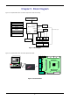
Chapter 5. Block Diagram Figure 5-1 is representative of the CPU board components and their connectivity.
Chapter 6. User Circuitry 6.1. Switches There are four switches located on the RSK. The function of each switch and its connection are shown in Table 6-1. Switch Function Microcontroller RES When pressed the RSK microcontroller is reset. RESn SW1/BOOT* Connects to an IRQ input for user controls. INT0 Pin18 The switch is also used in conjunction with the RES switch to place (Port 8, pin 2) the device in BOOT mode when not using the E8 debugger. SW2* Connects to an IRQ line for user controls.
6.4. Serial port The microcontroller programming serial port 1 is connected to the E8 connector. A serial port can be used by moving option resistors and fitting the D connector. This can be connected to serial channel 1 if the E8 is disabled from using channel 1; or serial channel 0 while the E8 is enabled.
6.5. LCD Module An LCD module is supplied to be connected to the connector J11. This should be fitted so that the LCD module lies over J3. Care should be taken to ensure the pins are inserted correctly into J11.The LCD module uses a 4 bit interface to reduce the pin allocation. No contrast control is provided; this is set by a resistor on the supplied display module. The module supplied with the RSK only supports 5V operation. Table 6-5 shows the pin allocation and signal names used on this connector.
6.6. Option Links Table 6-6 below describes the function of the option links contained on this RSK board. Option Link Settings Reference R14 Function Fitted Alternative (Removed) Related To Connects SCK to E8 SCK disconnected from E8 Programming Connects E8 to Programming MUST be removed if R44 fitted. R44 Serial Port Serial port. Programming Connects E8 to Programming Should be removed if R68 fitted. R68 Serial Port Serial port.
Option Link Settings Reference R100 Function Fitted Alternative (Removed) External Oscillator Connects External Ring header Disconnects sensitive pins to Microcontroller microcontroller signals from Related To R96 external pins. R97 External Oscillator Parallel resistor for crystal Not fitted R103 External Subclock Connects External Ring header Disconnects sensitive Oscillator pins to Microcontroller microcontroller signals from R105 external pins.
Option Link Settings Reference R109 Function VREF Fitted Alternative (Removed) Connects Board VCC1 VREF can be provided from supply to VREF external interface pins. (Fit Related To JA1,R110 R110) R110 VREF VREF to Application headers R109 should be fitted R109 R35 SW3 Connects SW3 to Analogue Disconnected R34 Trigger input R34 SW3 Connects SW3 to INT2 input Disconnected R35 R82 Microcontroller pin Connects microcontroller pin MUST be removed if R80 fitted.
Option Link Settings Reference R85 R88 R86 R128 R130 R118 R116 R131 R129 R117 R119 R67 R66 R45 R46 Function Fitted Alternative (Removed) Microcontroller pin Connects microcontroller pin Should be removed if R87 function select 24 to Wp pin fitted. Microcontroller pin Connects microcontroller pin 23 MUST be removed if R86 function select to TA2IN pin fitted. Microcontroller pin Connects microcontroller pin Should be removed if R88 function select 23 to Wn pin fitted.
6.7. Oscillator Sources A crystal oscillator is fitted on the RSK and used to supply the main clock input to the Renesas microcontroller. Table 6-7 details the oscillators that are fitted and alternative footprints provided on this RSK: Component Crystal (X1) Fitted 10MHz (HC/49U package) Subclock (X2) Fitted 32.768kHz (90SMX package) Table 6-7: Oscillators / Resonators 6.8. Reset Circuit The CPU Board includes a simple latch circuit that links the mode selection and reset circuit.
Chapter 7. Modes The RSK supports Boot mode and Single chip mode. Details of programming the FLASH memory is described in the M16C/6NK Group Hardware Manual. 7.1. Boot mode The boot mode settings for this RSK are shown in Table 7-1: Boot Mode pin settings below: CNVSS P5.0 P5.5 LSI State after Reset End 1 1 0 Boot Mode Table 7-1: Boot Mode pin settings The software supplied with this RSK only supports Boot mode using an E8 and HEW.
Chapter 8. Programming Methods The board is intended for use with HEW and the supplied E8 debugger. Refer to the M16C/6NK Group Hardware Manual for details of programming the microcontroller without using these tools.
Chapter 9. Headers 9.1. Microcontroller Headers Table 9-1 to Table 9-4 show the microcontroller pin headers and their corresponding microcontroller connections. The header pins connect directly to the microcontroller pins. * Marked pins are subject to option links.
J3 Pin Circuit Net Name Device Pin Circuit Net Name Pin Device Pin 1 A19_LED3 49 2 A18_LED2 50 3 A17_LED1 51 2 A16_LED0 52 5 A15_IO7 53 6 A14_IO6 54 7 A13_IO5 55 8 A12_IO4 56 9 A11_IO3 57 10 A10_IO2 58 11 A9_IO1 59 12 UC_VCC2 60 13 A8_IO0 61 14 GROUND 62 15 A7_DLCD7 63 16 A6_DLCD6 64 17 A5_DLCD5 65 18 A4_DLCD4 66 19 A3 67 20 A2 68 21 A1_DLCDE 69 22 A0_DLCDRS 70 23 D15 71 24 D14 72 25 D13 73 26 D12 74 27 D11 75 28 D10 7
9.2. Application Headers Table 9-5 and Table 9-6 below show the standard application connections. * Marked pins are subject to option links.
Table 9-7 to Table 9-9 below show the optional generic header connections. * Marked pins are subject to option links.
JA5 Pin Header Name RSK Signal Device Name Pin Pin Header Name RSK Signal Device Name Pin 1 ADC4 I4 AN4* 90 2 ADC5 I5 AN5* 89 3 ADC6 I6 AN6* 88 4 ADC7 I7 AN7* 97 5 CAN CAN0OUT 22 6 CAN CAN0IN 21 7 CAN CAN1OUT 99 8 CAN CAN1IN 100 9 Reserved 10 Reserved 11 Reserved 12 Reserved 13 Reserved 14 Reserved 15 Reserved 16 Reserved 17 Reserved 18 Reserved 19 Reserved 20 Reserved 21 Reserved 22 Reserved 23 Reserved 24 Reserved Table 9-8: J
Table 9-10 below shows the CAN connections J14 Pin Function 1 CAN0 Positive 2 GROUND 3 CAN0 Negative Signal Name Device Pin CAN0H 21 CAN0L 22 J15 Pin Function 1 CAN1 Positive 2 GROUND 3 CAN1 Negative Signal Name Device Pin CAN1H 100 CAN1L 99 Table 9-10: CAN Headers 22
Chapter 10. Code Development 10.1. Overview Note: For all code debugging using Renesas software tools, the RSK board must be connected to a PC USB port via an E8. An E8 is supplied with the RSK product. 10.2. Mode Support HEW connects to the Microcontroller and programs it via the E8. Mode support is handled transparently to the user. 10.3. Breakpoint Support HEW supports breakpoints on the user code, both in RAM and ROM. Double clicking in the breakpoint column in the code sets the breakpoint.
10.4.
Chapter 11.
Chapter 12. Additional Information For details on how to use High-performance Embedded Workshop (HEW, refer to the HEW manual available on the CD or from the web site. For information about the M16C/6NK series microcontrollers refer to the M16C/6NKGroup Hardware Manual For information about the M16C/6NK assembly language, refer to the M16C SeriesSoftware Manual. Online technical support and information is available at: http://www.renesas.
Renesas Starter Kit for M16C/6NK User's Manual Publication Date Rev.01.00 28.06.2006 Published by: Renesas Technology Europe Ltd. Duke’s Meadow, Millboard Road, Bourne End Buckinghamshire SL8 5FH, United Kingdom ©2006 Renesas Technology Europe and Renesas Solutions Corp., All Rights Reserved.
Renesas Starter Kit for M16C/6NK User's Manual Renesas Technology Europe Ltd.