
User's Manual

Rev.2.00 Nov 28, 2005 page 302 of 378
REJ09B0124-0200
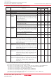
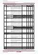
M16C/6N Group (M16C/6NK, M16C/6NM) 22. Electric Characteristics (Normal-ver.)
Under development
This document is under development and its contents are subject to change.
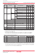
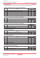
td(BCLK-AD)
th(BCLK-AD)
th(RD-AD)
th(WR-AD)
td(BCLK-CS)
th(BCLK-CS)
td(BCLK-ALE)
th(BCLK-ALE)
td(BCLK-RD)
th(BCLK-RD)
td(BCLK-WR)
th(BCLK-WR)
td(BCLK-DB)
th(BCLK-DB)
td(DB-WR)
th(WR-DB)
td(BCLK-HLDA)
ns
ns
ns
ns
ns
ns
ns
ns
ns
ns
ns
ns
ns
ns
ns
ns
ns
Address output delay time
Address output hold time (refers to BCLK)
Address output hold time (refers to RD)
Address output hold time (refers to WR)
Chip select output delay time
Chip select output hold time (refers to BCLK)
ALE signal output delay time
ALE signal output hold time
RD signal output delay time
RD signal output hold time
WR signal output delay time
WR signal output hold time
Data output delay time (refers to BCLK)
Data output hold time (refers to BCLK)
(3)
Data output delay time (refers to WR)
Data output hold time (refers to WR)
(3)
__________
HLDA output delay time
Symbol
Parameter
Min.
Standard
Unit
Max.
4
0
(NOTE 1)
4
–4
0
0
4
(NOTE 2)
(NOTE 1)
Switching Characteristics
(Referenced to VCC = 5V, VSS = 0 V, at Topr = –40 to 85 °C unless otherwise specified)
Table 22.25 Memory Expansion Mode and Microprocessor Mode (for setting with no wait)
25
25
15
25
25
40
40
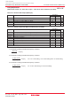
NOTES:
1. Calculated according to the BCLK frequency as follows:
0.5 ✕ 10
9
f(BCLK)
– 10 [ns]
2. Calculated according to the BCLK frequency as follows:
0.5 ✕ 10
9
f(BCLK)
– 40 [ns]
3. This standard value shows the timing when the
output is off, and does not show hold time of
data bus.
Hold time of data bus varies with capacitor volume
and pull-up (pull-down) resistance value.
Hold time of data bus is expressed in
t = – CR ✕ ln (1 – VOL / VCC)
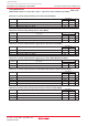
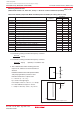
by a circuit of the right figure.
For example, when VOL = 0.2 VCC, C = 30 pF,
R =1 kΩ, hold time of output “L” level is
t = – 30 pF ✕ 1 kΩ ✕ ln (1 – 0.2 VCC / VCC) = 6.7 ns.
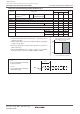
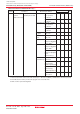
Figure 22.3 Port P0 to P14 Measurement Circuit
DBi
R
C
30pF
P0
P1
P2
P3
P4
P5
P6
P7
P8
P9
P10
P11
P12
P13
P14
NOTE:
1. P11 to P14 are only in the 128-pin version.
Measuring
condition
Figure 22.3
f(BCLK) is 12.5 MHz or less.
VCC = 5V