M34519T-MCU MCU Board for 4500 Series 4518, 4519, 4583 and 4584 Group MCUs User's Manual Rev.2.
* IBM and PC/AT are registered trademarks of International Business Machines Corporation. * NQPACK, YQPACK, YQSOCKET, YQ-Guide, HQPACK, TQPACK and TQSOCKET are trademarks of Tokyo Eletech Corporation. Keep safety first in your circuit designs! • Renesas Technology Corporation and Renesas Solutions Corporation put the maximum effort into making semiconductor products better and more reliable, but there is always the possibility that trouble may occur with them.
Preface This user's manual describes the specifications of MCU board M34519T-MCU for the Renesas 4518, 4519, 4583 and 4584 Groups of 4-bit CMOS single-chip MCUs. The M34519T-MCU is an MCU board for the PC4504 emulator. For emulator main unit PC4504 and emulator debugger M3T-PD45, refer to each user's manual (online manual).
Contents Chapter 1. Precautions for Safety ........................................................................................... 5 1.1 Safety Symbols and Meanings .............................................................................. 5 Chapter 2. Package Contents .................................................................................................. 9 2.1 Contents of the M34519T-MCU ........................................................................... 9 2.
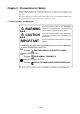
Chapter 1. Precautions for Safety Both in the M34519T-MCU user's manual and on the product, several icons are used to insure proper handling of this product and also to prevent injuries to you or other persons, or damage to your properties. This chapter describes precautions which should be taken in order to use the M34519T-MCU safely and properly. Be sure to read this chapter before using this product. 1.
WARNING Warning for Installation: • Do not set this product in water or areas of high humidity. Spilling water or some other liquid into the main unit can cause an unrepairable damage. Warning for Use Environment: • This equipment is to be used in an environment with a maximum ambient temperature of 35°C. Care should be taken that this temperature is not exceeded. CAUTION Cautions to Be Taken for This Product: • Do not disassemble or modify this product.
IMPORTANT Notes on Connecting the Target System: • When connecting the target system, be sure to shut off the power of the emulator and the target system. • Connect the emulator probe carefully. • When connecting the emulator probe, use care not to twist the cable. An excessive twist may cause breaking of the wire. Note on MCU board Installation: • Before installing and removing the MCU board, always be sure to power off the PC4504 emulator main unit and unplug its power cord from the outlet.
MEMO ( 8 / 36 )
Chapter 2. Package Contents 2.1 Contents of the M34519T-MCU Table 2.1 shows the contents of the M34519T-MCU package. When unpacking it, check to see that all of these components are included. Table 2.
2.2 Other Necessary Products To bring forward your program development with the 4518, 4519, 4583 and 4584 Groups of 4-bit MCUs, the products listed in Table 2.2 are necessary in addition to those contained in the package. Get them separately when necessary. Table 2.
Chapter 3. M34519T-MCU 3.1 Outline With emulator main unit PC4504, the M34519T-MCU can make up an emulator system which can be operated by a host machine. Figure 3.1 shows an emulator system configuration. For details on how to connect the target system, refer to "3.6 Connection to the Target System" (page 18).
3.2 Specifications Table 3.1 lists specifications of the M34519T-MCU. Table 3.1 M34519T-MCU specifications Emulator Emulator PC4504 Applicable MCUs 4518 Group, 4519 Group, 4583 Group*1, 4584 Group*1 Evaluation MCU 4518, 4519 Groups M34519M8-001FP (preinstalled) 4583, 4584 Groups M34584MD-001FP (included) Monitor program 4518, 4519 Groups M4519 (preinstalled) 4583, 4584 Groups M4584 (included) Clock Main clock: 6.0 MHz (OSC-2 [6.
3.3 Switches Table 3.2 shows the functions of the switches and their factory-settings. Table 3.2 Functions of the switches Switch Description Switch position Label OFF ON OFF Does not output VDD from the M34519T-MCU to the target system. ON ON OFF Outputs VDD from the M34519T-MCU to the target system. Factory-setting SW1 OFF Set the MCU's ROM size.
3.4 Check Pins Table 3.3 lists the check pins of the M34519T-MCU, and Figure 3.3 shows their positions. Table 3.3 Check pins Function Pin TP1 VDD Outputs +3 V or +5 V (MCU voltage) according to the setting of SW3. TP2 XIN Outputs a system clock input to the evaluation MCU. TP3 GND Ground TP4 RUN/STOP Held low when a user program is executed, held high when it is stopped.
(1) Connector J3 Table 3.5 lists the pin assignments of the 100-wire half-pitch connector J3 for connecting the PCA4029. And Figure 3.4 shows the pin layout of connector J3. Table 3.5 Pin assignments of connector J3 Line A Pin No. Signal 1 Line B I/O Pin No. Signal GND 1 2 GND 3 GND 4 Line C Line D Pin No. Signal I/O Pin No.
Some signals which are connected to the target system are emulated by the M34519T-MCU. Table 3.6 lists the connections of the target system and each pin. Table 3.
(3) Connector J6 Connector J6 is a connector used to connect oscillator circuit board OSC-2. Table 3.8 lists the pin assignments of connector J6. Figure 3.5 shows the pin layout of connector J6. Figure 3.6 shows a connection diagram of oscillator circuit board OSC-2 (6.0 MHz). Table 3.8 Pin assignments of connector J6 Pin No. Signal Function 1 VCC Power supply 2 GND GND 3 CLK Clock input 4 GND GND Figure 3.5 Pin layout of connector J6 Figure 3.
3.6 Connection to the Target System Connections of the M34519T-MCU and target systems are shown in Figure 3.7 below. 50-wire normal-pitch cable M34513T-PTCA M34513T-PTCA M34513T-PTCB M34513T-PTCC TQPACK032SA FFC-50BSM1 (1) Connection to 2.54-mm-pitch 50-pole dual-in-line pin ME-2-1 (2) Connection to IC socket for 32-pin SDIP Figure 3.
(1) Connection to 2.54-mm-pitch 50-pole dual-in-line pins (for 42-pin SSOP) Connect this product to 50-pole dual-in-line pins using the included 50-wire normal-pitch cable. Use the following products: (1) 100-wire half-pitch cable (40 cm) (2) Pitch converter board PCA4029 (3) 50-wire normal-pitch cable (10 cm) Table 3.9 lists the connector assignments of the 50-wire normal-pitch cable, and Figure 3.8 shows the pin layout of the 50-wire normal-pitch cable.
(2) Connection to the IC socket for 32-pin SDIP Attach pitch converter board M34513T-PTCA to the 50-wire normal-pitch cable, and connect it to an IC socket for 32-pin SDIP on the target system. Use the following products: (1) 100-wire half-pitch cable (40 cm) (2) Pitch converter board PCA4029 (3) 50-wire normal-pitch cable (10 cm) (4) Pitch converter board M34513T-PTCA Table 3.10 lists the connector assignments of pitch converter board M34513T-PTCA. When attaching the pitch converter board, check the No.
(3) Connection to a 32-pin LQFP foot pattern Attach pitch converter boards M34513T-PTCA and M34513T-PTCB to the included 50-wire normal-pitch cable, and connect them to the TQPACK032SA soldered on a 32-pin LQFP foot pattern of the target system via the M34513T-PTCC.
3.7 How to Replace the MCU For debugging the 4583 and 4584 Group MCUs, it is necessary to replace the evaluation MCU to the included M34584MD-001FP. When replacing the MCU, match the No. 1 pin of the IC socket and that of the MCU as shown in Figure 3.10. Incorrect insertion may cause a fatal damage to the MCU. The M34519M8-001FP is mounted when shipped from the factory. Top view 42 22 M34584MD-001FP 1 21 Figure 3.
Chapter 4. Precautions to Be Taken for Debugging a Program 4.1 Reset The M34519T-MCU uses a 74HC14 for its RESET signal input buffer, so that its electrical characteristics differ from those of an actual MCU. Table 4.1 lists the RESET signal input characteristics of the M34519T-MCU. Table 4.1 RESET signal input characteristics Item H-level threshold voltage L-level threshold voltage Hysteresis voltage Symbol VP VN VH Voltage Min. Max. VCC = 2.0 V 1.0 V 1.5 V VCC = 4.5 V 2.3 V 3.
4.3 RAM Backup Mode In RAM backup mode, the M34519T-MCU operates differently from the actual MCUs. Although the actual MCU enters RAM backup mode depending on a combination of instructions EPOF and POF, the M34519T-MCU is placed in RAM backup mode by executing instruction POF only. Instruction EPOF has no effect on the M34519T-MCU. [Actual MCU] Program example 4.1 Placed in RAM backup mode RC INY EPOF POF • • [M34519T-MCU] Placed in RAM backup mode [Actual MCU] Program example 4.
(3) Port I/O Characteristics With the M34519T-MCU, port I/O characteristics are different from actual MCUs because there are emulation circuits in ports P00--P03, P10--P13 and D0--D5. Table 4.2 lists port I/O characteristics of the M34519T-MCU. Table 4.2 Emulation port I/O characteristics Port Device Item Condition Min. Standard Max. VCC = 2.0 V 1.50 V - - VCC = 4.5 V 3.15 V - - VCC = 2.0 V - - 0.50 V VCC = 4.5 V - - 1.35 V VOL VCC = 4.5 V - 0.35 V 0.5 V IOL VCC = 5.
4.6 System Clock Depending on the supply voltage and operation mode, use one of the following frequencies listed in Table 4.3. Table 4.3 M34519T-MCU operating frequencies Voltage Mode Frequency Divide-by-8 Divide-by-4 6.0 MHz or less 5V Divide-by-2 Through Divide-by-8 Divide-by-4 6.0 MHz or less 3V Divide-by-2 Through 4.4 MHz or less To change a clock frequency, attach the necessary parts to the included oscillator circuit board OSC-2.
4.9 Program Execution (G, GB) The PC4504 and M34519T-MCU's hardware is subject to the following restrictions with respect to the operation of the program execution commands (G and GB). (1) Continuous description of instructions Hardware breakpoints set in a continuous description of instructions following one after another do not cause a break to occur in the continuous description of instructions.
4.10 External Trigger Signal (1) External trigger signal input timing The latch timing of the external trigger signal is shown in Figure 4.3. Instruction Next Instruction System clock XIN External trigger signal TRIG Figure 4.3 Latch timing of the external trigger signal (2) External trigger signal input characteristics Trigger breaks work according to the conditions (leading edge/trailing edge) of signals input from the external trigger cable.
Chapter 5. Connection Circuit Diagrams 5.1 Connection Circuit Diagrams Figures 5.1 and 5.2 show the connection circuit diagrams of the M34519T-MCU. These circuit diagrams depict the M34519T-MCU connection centering on circuits connected to the target system. Emulator control blocks and other similar circuits that are not connected to the target system are omitted in this diagram. : denotes control signal Figure 5.
: denotes control signal Figure 5.
Chapter 6. Pitch Converter Board External Dimensions 6.1 M34513T-PTCA Figure 6.1 shows external dimensions of the M34513T-PTCA. Unit: mm Figure 6.1 External dimensions of the M34513T-PTCA 6.2 M34513T-PTCB Figure 6.2 shows external dimensions of the M34513T-PTCB. Unit: mm Figure 6.2 External dimensions of the M34513T-PTCB 6.3 M34513T-PTCC Figure 6.3 shows external dimensions of the M34513T-PTCC. Unit: mm Figure 6.
MEMO ( 32 / 36 )
Chapter 7. Maintenance and Guarantee 7.1 Maintenance If dust or dirt collects on any equipment of your emulation system, wipe it off with a dry soft cloth. Do not use thinner or other solvents because these chemicals can cause the equipment's surface coating to separate. 7.
7.4 How to Request for Repair If your M34519T-MCU is found faulty, follow the procedure below to send your product for repair. Customer Fill in the Repair Request Sheet included with this product, then send it along with this product for repair to your local distributor. Make sure that information in the Repair Request Sheet is written in as much detail as possible to facilitate repair.
M34519T-MCU User's Manual Rev.2.