
User manual


Rev. 1.00, 05/04, page 152 of 544
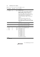
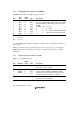
8.3.4 PWM Output Enable Register A (PWOERA)
PWOERA switches between PWM output and port output.
Bit
Bit
Name
Initial
Value
R/W Description
7
6
5
4
3
2
1
0
OE7
OE6
OE5
OE4
OE3
OE2
OE1
OE0
0
0
0
0
0
0
0
0
R/W
R/W
R/W
R/W
R/W
R/W
R/W
R/W
Output Enable 7 to 0
These bits, together with P1DDR, specify the P1n/PWn
pin state. Bits OE7 to OE0 correspond to outputs PW7
to PW0.
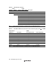
P1nDDR OEn: Pin state
0 x: Port input
1 0: Port output or PWM 256/256 output
1 1: PWM output (0 to 255/256 output)
[Legend]
x: Don't care
Note: n = 7 to 0
To perform PWM 256/256 output when DDR = 1 and OE = 0, the corresponding pin should be set
to port output.
DR data is output when the corresponding pin is used as port output. A value corresponding to
PWM 256/256 output is determined by the OS bit, so the value should have been set to DR
beforehand.
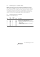
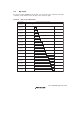
8.3.5 Peripheral Clock Select Register (PCSR)
PCSR selects the PWM input clock.
Bit Bit Name
Initial
Value R/W Description
7 to 4 All 0 R/W Reserved
These bits cannot be modified.
3
2
1
PWCKC*
PWCKB
PWCKA
0
0
0
R/W
R/W
R/W
PWM Clock Select C, B, A
Together with bits PWCKE and PWCKS in PWSL,
these bits select the internal clock input to the clock
counter in the PWM. For details, see table 8.2.
0 0 R/W Reserved
These bits cannot be modified.
Note: The program development tool (emulator) does not support this function.