
User manual


Rev. 1.00, 05/04, page 426 of 544
16.7.3 Setting Range of Analog Power Supply and Other Pins
If conditions shown below are not met, the reliability of this LSI may be adversely affected.
• Analog input voltage range
The voltage applied to analog input pin ANn during A/D conversion should be in the range
AVss ≤ ANn ≤ AVref (n = 0 to 5).
• Relation between AVcc, AVss and Vcc, Vss
For the relationship between AVcc, AVss and Vcc, Vss, set AVss = Vss. If the A/D converter
is not used, the AVcc and AVss pins must on no account be left open.
• AVref pin reference voltage specification range
The reference voltage of the AVref pin should be in the range AVref ≤ AVcc.
16.7.4 Notes on Board Design
In board design, digital circuitry and analog circuitry should be as mutually isolated as possible,
and layout in which digital circuit signal lines and analog circuit signal lines cross or are in close
proximity should be avoided as far as possible. Failure to do so may result in incorrect operation
of the analog circuitry due to inductance, adversely affecting A/D conversion values. Also, digital
circuitry must be isolated from the analog input signals (AN0 to AN5), analog reference voltage
(AV
ref
), and analog power supply (AV
CC
) by the analog ground (AV
SS
). Also, the analog ground
(AV
SS
) should be connected at one point to a stable digital ground (V
SS
) on the board.
16.7.5 Notes on Noise Countermeasures
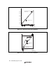
A protection circuit connected to prevent damage due to an abnormal voltage such as an excessive
surge at the analog input pins (AN0 to AN5) and analog reference voltage (AV
ref
) should be
connected between AVcc and AVss as shown in figure 16.8. Also, the bypass capacitors
connected to AVcc and AV
ref
, and the filter capacitor connected to AN0 to AN5, must be
connected to AV
SS
.
If a filter capacitor is connected, the input currents at the analog input pins (AN0 to AN5) are
averaged, and so an error may arise. Also, when A/D conversion is performed frequently, as in
scan mode, if the current charged and discharged by the capacitance of the sample-and-hold circuit
in the A/D converter exceeds the current input via the input impedance (R
in
), an error will arise in
the analog input pin voltage. Careful consideration is therefore required when deciding the circuit
constants.