
User manual


Rev. 1.00, 05/04, page 479 of 544
Section 21 List of Registers
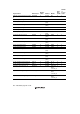
The register list gives information on the on-chip I/O register addresses, how the register bits are
configured, and the register states in each operating mode. The information is given as shown
below.
1. Register Addresses (address order)
• Registers are listed from the lower allocation addresses.
• The MSB-side address is indicated for 16-bit addresses.
• Registers are classified by functional modules.
• The access size is indicated.
2. Register Bits
• Bit configurations of the registers are described in the same order as the Register Addresses
(address order) above.
• Reserved bits are indicated by in the bit name column.
• The bit number in the bit-name column indicates that the whole register is allocated as a
counter or for holding data.
• 16-bit registers are indicated from the bit on the MSB side.
3. Register States in Each Operating Mode
• Register states are described in the same order as the Register Addresses (address order)
above.
• The register states described here are for the basic operating modes. If there is a specific reset
for an on-chip peripheral module, see the section on that on-chip peripheral module.
4. Register Select Conditions
• Register states are described in the same order as the Register Addresses (address order)
above.
• For details on the register select conditions, see section 3.2.2, System Control Register
(SYSCR), 3.2.3, Serial Timer Control Register (STCR), 20.1.3, Module Stop Control Registers
H, L (MSTPCRH, MSTPCRL), and the register descriptions for each module.