REG10J0020-0200 Renesas Starter Kit LCD Application Board User's Manual RENESAS STARTER KIT Rev.2.00 Revision date:29.11.2007 Renesas Technology Europe Ltd. www.renesas.
Table of Contents Chapter 1. Preface ..................................................................................................................................................3 Chapter 2. Purpose .................................................................................................................................................4 Chapter 3. Board Layout .........................................................................................................................................
Chapter 1. Preface Cautions This document may be, wholly or partially, subject to change without notice. All rights reserved. Duplication of this document, either in whole or part is prohibited without the written permission of Renesas Technology Europe Limited. Trademarks All brand or product names used in this manual are trademarks or registered trademarks of their respective companies or organisations. Copyright © Renesas Technology Europe Ltd. 2007. All rights reserved. Website: http://www.eu.renesas.
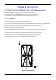
Chapter 2.Purpose This RSK Application Board is an evaluation tool for Renesas microcontrollers with an LCD driver interface. It is used in conjunction with the RSK for the microcontroller to be evaluated. Features include: • Mounting connections to allow RSK to be added to top of board. • Interface to standard RSK LCD expansion connector and RSK expansion connections. • 8 character 14 segment “starburst” LCD. • Coin cell holder to power mounted RSK for low power operation.
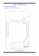
Chapter 3.Board Layout 3.1.Component References The following diagram shows the component references for the board.
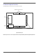
3.2.Board Component functions The following diagram the shows the functions of the components on the board. Application Board Interface JA5 JA1 LCD J A4 Switch JA6 Coin Cell Holder JA2 Application Board Interface LCD Application Interface Figure 3-2: Board Layout Caution: If processor is not in low power mode at start up the battery life will be significantly reduced.
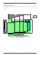
3.3.Board Dimensions The following diagram gives the board dimensions and connector positions. All through hole connectors are on a common 0.1” grid for easy interfacing. 170.00mm 115.00mm Corners x4 3mm radius 86.36mm 50.80 mm Coin Cell Holder JA5 JA1 Figure 3-3 : Board Dimensions 7 5.00mm 3.81mm 45.00mm LCD 100.00mm 85.00mm 14.00mm JA4 80.01mm LCD connector JA6 OFF JA2 ON 27.
Chapter 4.User Circuitry 4.1.Fitting the Target RSK to the RSK LCD application board The board is supplied with 2x 24 way sockets, 2x 26 way sockets and 1 x 50 way socket. These should be soldered on the underside of the host RSK in JA1, JA2, JA5, JA6 and JA4 positions. The RSK should be plugged into the equivalent connectors on the RSK LCD application board. 4.2.LCD Module The LCD module on the board is connected to the RSK LCD connector JA4. It uses ¼ duty cycle and has 4 common lines.
Segment Bit number L 7 K 6 J 5 I 4 DP 3 C 2 B 1 A 0 D 7 E 6 F 5 X 4 M 3 N 2 G 1 H 0 Hex value for RAM A B C D E F G H I J K L M N O P Q R T S U V W X Y Z 0 1 0 0 0 0 1 0 0 0 1 0 0 1 0 0 1 1 0 0 0 1 1 1 0 0 1 0 0 0 1 1 0 1 0 0 0 0 0 0 0 1 0 1 0 1 0 0 0 0 0 0 0 1 0 0 0 0 0 0 0 0 1 0 1 0 0 0 0 0 0 0 0 0 0 1 1 1 0 0 0 0 0 0 0 0 1 0 0 0 0 0 0 0 0 0 1 0 0 0 0 0 0 0 0 0 0 0 0 0 0 0 0 0 0 0 0 0 0 0 0 0 0 0 0 0 0 0 0 0 1 0 0 0 0 0 0 1 0 1 0 0 1 1 1 0 1 0 0 1 1 1 1 0 0 0 1 0 0 0 0 0 0 1 0 1 0
4.3.Coin Cell and switch. The board includes a coin cell holder to hold a 2032 3.6V coin cell. To power the attached RSK from this cell the switch must be in the “ON” position. IT IS IMPORTANT NOT TO POWER THE ATTACHED RSK VIA THE POWER SUPPLY JACK OR VIA THE E8A IF THIS OPTION IS USED. Caution: If processor is not in low power mode at start up the battery life will be significantly reduced. 4.4.Capacitors Pads are supplied to allow 0603 capacitors to be placed on the LCD drive voltages V1 – V4.
Chapter 5.Headers 5.1.Application Headers This information is supplied for reference. Only JA1 pin 3 (battery supply voltage to RSK) and the ground pins are connected on this board. Table 5-1 and Table 5-2 below show the standard application header connections.
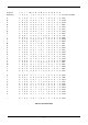
JA2 Pin Generic Header Name CPU board Pin Header Name Signal Name CPU board Signal Name 1 Open drain RESn 2 External Clock Input EXTAL 3 Open drain NMIn 4 Regulated Supply 1 Vss1 5 Open drain output WDT_OVF 6 Serial Port SCIaTX IRQ0 8 Serial Port SCIaRX 7 Open drain WUP 9 Open drain IRQ1 10 Serial Port SCIaCK 11 Up/down MO_UD 12 Serial Port Handshake CTS/RTS 13 Motor control MO_Up 14 Motor control MO_Un 15 Motor control MO_Vp 16 Motor control MO_Vn 17
JA6 Pin Generic Header Name CPU board Pin Header Name Signal CPU board Signal Name Name 1 DMA DREQ 2 DMA DACK 3 DMA TEND 4 Standby (Open drain) STBYn 5 Host Serial RS232TX 6 Host Serial RS232RX 7 Serial Port SCIbRX 8 Serial Port SCIbTX 9 Serial Port Synchronous SCIcTX 10 Serial Port SCIbCK 11 Serial Port Synchronous SCIcCK 12 Serial Port 13 Reserved 14 Reserved 15 Reserved 16 Reserved 17 Reserved 18 Reserved 19 Reserved 20 Reserved 21 Reserved 22
Table 5-5 below shows the LCD header connections JA4 Pin Generic Header Name Signal Name Pin Header Name 1 V0 V0 2 V1 V1 3 V2 V2 4 V3 V3 5 GROUND GROUND 6 GROUND GROUND 7 COM1 COM1 8 COM2 COM2 9 COM3 COM3 10 COM4 COM4 11 SEG1 SEG1 12 SEG2 SEG2 13 SEG3 SEG3 14 SEG4 SEG4 15 SEG5 SEG5 16 SEG6 SEG6 17 SEG7 SEG7 18 SEG8 SEG8 19 SEG9 SEG9 20 SEG10 SEG10 21 SEG11 SEG11 22 SEG12 SEG12 23 SEG13 SEG13 24 SEG14 SEG14 25 SEG15 SEG15 26 SEG
Chapter 6.Code Development RSKs with appropriate LCD connections will include suitable sample software to drive the LCD on this board. Section 4.2 includes details of bit mapping for the LCD segments.
Chapter 7.Additional Information For details on how to use High-performance Embedded Workshop (HEW), refer to the HEW manual available on the CD or from the web site. Online technical support and information is available at: http://www.renesas.com/renesas_starter_kits Technical Contact Details America: techsupport.rta@renesas.com Europe: tools.support.eu@renesas.com Japan: csc@renesas.com General information on Renesas Microcontrollers can be found on the Renesas website at: http://www.renesas.
Renesas Starter Kit LCD Application Board User's Manual Publication Date Rev.2.00 29.11.2007 Published by: Renesas Technology Europe Ltd. Duke’s Meadow, Millboard Road, Bourne End Buckinghamshire SL8 5FH, United Kingdom ©2007 Renesas Technology Europe and Renesas Solutions Corp., All Rights Reserved.
Renesas Starter LCD Application Board User's Manual Renesas Technology Europe Ltd.