Applications Engineering ZigBee Demo Kit (ZDK) RZB-ZMD16C-ZDK User’s Manual Version 1.2 August 2006 www.renesas.
Applications Engineering Table of Contents 1.0 Introduction ............................................................................................................................................. 4 2.0 Contents of Product Package................................................................................................................. 5 2.1. RZB-ZMD16C-ZDK ZigBee Demonstration Kit Item List................................................................... 5 2.2. CD-ROM ........................
Applications Engineering 8.3. Operating Environment.................................................................................................................... 20 Appendix A. Troubleshooting Guide........................................................................................................... 21 A.1 Manual Installation ........................................................................................................................... 21 A.2 USB Driver Problems .....................
Applications Engineering 1.0 Introduction The RZB-ZMD16C-ZDK kit is a low-cost ZigBee demonstration kit for evaluating wireless ZigBee connectivity solutions based on the Renesas M16C/28 group of microcontrollers (MCU). A small ZigBee Personal Area Network (PAN) can be set up, monitored and analyzed with the included hardware and software.
Applications Engineering 2.0 Contents of Product Package This section describes the contents of the RZB-ZMD16C-ZDK product package. When unpacking your RZB-ZMD16C-ZDK, please check to see that all items listed below are included. 2.1. RZB-ZMD16C-ZDK ZigBee Demonstration Kit Item List Table 2-1 lists the items included in the RZB-ZMD16C-ZDK.
Applications Engineering 3.0 Limited Guarantee and Support Renesas Technology America, Inc., warrants the RZB-ZMD16C-ZDK to be free from component or assembly defects for a period of 180 days from the date of purchase. Settlement is limited to repair or replacement of the product only. Renesas Technology America, Inc., does not assume any liability arising out of the application or use of any product, circuit or procedure described herein. No other liability or warranty applies, expressed or implied.
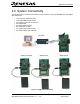
Applications Engineering 4.0 System Connectivity The following lists the hardware and software products required for using the RZB-ZMD16C-ZDK ZigBee Demonstration Kit. • • • • • • • • Host Computer (supplied by user) Three RZB-ZMD16C-ZDK Boards Three battery packs with AA batteries RF Sniffer Board RF Sniffer Interface (RFSI) Mini USB cable for RFSI 2×5 header target cable for RFSI RF Sniffer software and USB driver RF Sniffer ZigBee Coordinator ZigBee Router ZigBee Router Figure 4.
Applications Engineering Optional (only required if you want to update firmware and/or develop code). • • • • In-Circuit Debugger and Programmer (ICD) Mini USB cable for ICD 2×5 header target cable for ICD Software Tools (HEW IDE, NC30 Compiler/Linker, FoUSB Programmer) Figure 4-2 shows an ICD unit connected to a PC via USB and to a ZDK board via 2×5-pin ribbon cable. Figure 4-2 ZDK Development System Connectivity 4.1.
Applications Engineering on the board hardware, and the RF Sniffer User’s Manual for more information on RF Sniffer usage and features. 4.4. RF Sniffer Interface (RFSI) The RF Sniffer interface is an RTA-FoUSB-MON unit that comes pre-programmed with firmware to allow the RF Sniffer software running on the Host PC to take control of the RF Sniffer board. The RFSI connects to the PC’s USB port via the included mini USB cable, and to the RF Sniffer board via the included 2×5-header ribbon cable.
Applications Engineering *Note: The number of breakpoints will vary depending on the M16C flash MCU used. 4.7.4. FoUSB (Flash-over-USB™) Programmer The Flash Over USB Programmer application provides In-System Programming capability for the starter kit or any target board using an M16C family flash MCU (e.g. R8C, M16C, M32C). Please see the RTA-FoUSB-MON User’s Manual for more details. RZB-ZMD16C-ZDK User’s Manual Rev 1.
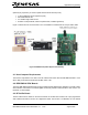
Applications Engineering 5.0 Hardware 5.1. ZDK Board (RZB-ZMD16C-ZDK) Note:The RZB-ZMD16C-ZDK board is referred to as RZB-ZMD28-BRD on the board's silkscreen and schematic drawing. Figure 5-1 shows the RZB-ZMD16C-ZDK Board with major components identified. Figure 5.1: RZB-ZMD16C-ZDK Board RZB-ZMD16C-ZDK User’s Manual Rev 1.
Applications Engineering 5.2. RZB-ZMD16C-ZDK Board Block Diagram The RZB-ZMD16C-ZDK board incorporates an M30280FAHP (80-pin QFP) from the M16C/28 group of microcontrollers designated as U4. Figure 5-2 shows the RZB-ZMD16C-ZDK block diagram. Y1 10MHz Y2 S1 S2 P10_4 8 characters x 2 lines LCD P0_0...
Applications Engineering 5.4.2. JP2: Power LED (D4) and RS232 (U7) Transceiver Power JP2 is used to connect the Vcc pin of the RS232 transceiver chip (U7) to the 3.3V supply of the board. It also connects the red Power LED (D4) to the board’s supply. It can be used to reduce the board’s power consumption by disconnecting the RS232 transceiver and Power LED. For normal operations, JP2 must be shorted. JP2 is shorted by default. 5.4.3.
Applications Engineering 6.2. System Clock After reset, the main system clock (denoted in the spec as f1) is set up to run at 20MHz. The ZigBee stack assumes that the MCU is running at this operating frequency. Please do not make any changes to the clock. 6.3. Interrupts The interrupt vector table is located in the ZigBee stack and real-time operating system (RTOS) program memory area (ZbROM). Therefore, you cannot implement any interrupt sub-routines other than the ones listed below.
Applications Engineering 6.6. Global Variable RAM Usage You may create as many global variables for your user program as RAM space is available (896 bytes). A virtual RAM section at the start of the debugger’s RAM has been created to warn you if you try to allocate too much global RAM. Below is an example of the linker warning you will receive if you exceed the available RAM space: Phase M16C Linker starting C:\WorkSpace\test\test\sect30_zdk28.
Applications Engineering 6.11. Customization of Demo Program Settings The following definitions can be changed at the top of the ZDK_Demo.c file to fit your requirements.
Applications Engineering 7.0 System Operation & Limitations The RZB-ZMD16C-ZDK provides sophisticated debugging features at a low cost, but it does have some limitations when used with the debugger and ICD. Section 6.1 introduces the kernel (ROM monitor) program and its purpose. The limitations when this kernel is running with the user program are listed in Table 7-1. Table 7-1: System Limitations when Debugging Item Please Refer To 7.2 Pin and Peripheral Limitations 7.3 Memory Map User Limitations 7.
Applications Engineering 00000h 00400h 023FFh SFR Area 00400h User RAM Area = 8064 Bytes 0237Fh 02380h Kernel RAM Internal RAM Area - 8kB (128 Bytes) Reserved 0F000h 0F800h 10000h High E/W 2kB data block 023FFh Note: User programs must not use shaded areas.
Applications Engineering Table 7-3: Interrupt Vector Addresses Interrupt Cause M16C/28 Vector Address Undefined FFFDCh ~ FFFDFh Overflow FFFE0h ~ FFFE3h BRK Instruction FFFE4h ~ FFFE7h Address Match FFFE8h ~ FFFEBh Single-step FFFECh ~ FFFEFh Watchdog Timer FFFF0h ~ FFFF3h DBC FFFF4h ~ FFFF7h NMI FFFF8h ~ FFFFBh RESET FFFFCh ~ FFFFFh Kit Specification User available User available User inhibited User inhibited User inhibited User available (Note 1) User inhibited User available Reset vector (Note 2) NOTE
Applications Engineering 8.0 RZB-ZMD16C-ZDK Board Specifications 8.1. Hardware Specifications Table 8-1 lists the specifications of the RZB-ZMD16C-ZDK Board. Table 8-1: RZB-ZMD16C-ZDK Board Specifications Item Specification MCU M30280FAHP Clocks Main Clock: crystal 10 MHz, PLL, or ring oscillator Sub Clock: 32.
Applications Engineering Appendix A. Troubleshooting Guide This section discusses possible problems you may encounter while installing the development tool software, USB drivers, or running the HEW debugger and FoUSB Programmer applications. This section also discusses the countermeasures and solutions to resolve these problems. For troubleshooting information on the RF Sniffer Interface and RF Sniffer board, see the RF Sniffer User’s Manual.
Applications Engineering If you encounter problems on installing the drivers, you can try the following: Windows 2000 a. Copy the fousb.inf and usbmon.inf files from the C:\Renesas\FoUSB\USB Drivers folder to the \WINNT\INF folder. b. Copy the fousb.sys and usbmon.sys files from the C:\Renesas\FoUSB\USB Drivers folder to the \WINNT\SYSTEM32\drivers folder. Windows 98 or XP a. Copy the fousb.inf and usbmon.inf files from the C:\Renesas\FoUSB\USB Drivers folder to the \WINDOWS\INF folder. b. Copy the fousb.
Applications Engineering • USB was not selected on the HEW Init dialog box. Please select ‘USB’ from the Init dialog box that is displayed right after you start a debug session. • The selected MCU on the ICD board and the actual target MCU (M16C/28) do not match. Close the error message by clicking on the ‘OK’ button, then click on the ‘Cancel’ button of the Init window. Make sure you select ‘M30280FA.mcu’. If the MCU loaded on the ICD is different, HEW will re-program the ICD to match it.
Applications Engineering • • Press the reset button on the ZDK board. Click the HEW Reset icon. After initialization, debugging can resume. However, it is recommended that you download your program again before debugging. RZB-ZMD16C-ZDK User’s Manual Rev 1.
Applications Engineering Appendix B. Reference Manuals Item Title Description 1. Renesas ZigBee Demonstration Kit (ZDK)Quick Start Guide Document that will help you get started on using the ZigBee Demonstration Kit. 2. 3. RZB-ZMD16C-ZDK User’s Manual RF Sniffer User's Manual 4. ZDK Board Schematic 5. 6. 8. ZDK Board BOM M16C/20/60 Series C-Language Programming Manual M16C/20/60 Series Assembler Language Programming Manual HEW User's Manual 9. 10. 11.
Applications Engineering Appendix C. Expansion Headers The M30280FA MCU on the RZB-ZMD16C-ZDK target board is housed in an 80-pin QFP package. Pin 1 of the package is identified by a little white circle on the board’s top silkscreen. Connectors J1 to J4, located around the MCU, provide access to almost all of the MCU’s pins. You can use J1-J4 as test points to check MCU signals or, by mounting your own headers, connect your own expansion board.
Applications Engineering J3 Pin 1 2 3 MCU Pin 41 42 43 J4 Pin 1 2 3 MCU Pin 61 62 63 4 5 6 7 8 44 45 46 47 48 P62/RxD0 P61/CLK0 P60/ CTS 0 / RTS 0 P27/OUTC17/INPC17 P26/OUTC16/INPC16 P25/OUTC15/INPC15 P24/OUTC14/INPC14 P23/OUTC13/INPC13 P06/AN06 P05/AN05 P04/AN04 4 5 6 7 8 64 65 66 67 68 P03/AN03 P02/AN02 P01/AN01 P00/AN00 P107/AN7/ KI3 9 49 P22/OUTC12/INPC12 9 69 P106/AN6/ KI2 10 50 P21/OUTC11/INPC11/SCLMM 10 70 P105/AN5/ KI1 11 51 P20/OUTC10/INPC10/SDAMM 11 71 12 52 P17/ INT
Applications Engineering Appendix D. Board Schematic & BOM Note:The RZB-ZMD16C-ZDK board is referred to as RZB-ZMD28-BRD on the board's silkscreen and schematic drawing. The circuit board schematic and Bill-Of-Materials (BOM) are available as separate PDF documents. They can be accessed through Start > Programs > Renesas > RZB_ZMD16C_ZDK > Board Hardware, or by browsing to the folder C:\Renesas\RZB_ZMD16C_ZDK\Docs\ ZDK_Manuals and opening the files: RZB_ZMD28_BRD_BOM.pdf RZB_ZMD28_BRD_Schematic.
A B C D 5 9 4 8 3 7 2 6 1 TP1 GND Point R31 10K POT_EN 2 C25 0.1uF Tip 6 4 1 2 3 1 R1IN R2IN T1OUT T2OUT V- V+ 5 2 R44 10K 1 2 MAX202 R1OUT 12 R2OUT 9 T1IN 11 T2IN 10 5 C1- 3 C2+ 4 C1+ 1 C2- R10 10K 2 TEMP_EN U3-1 NDS9956A RT1 t 10K R30 10K 4 RS232_IN CDS_EN U8-2 NDS9956A R3 CdS Cell AN0 AN1 AN2 0 R33 R17 10K 0 0 R39 R37 C23 0.1uF C21 0.1uF S1 4 S2 DVDD_3.
A B C 5 FIDUCIAL FIDUCIAL 1 1 1 1 F2 R47 R18 R20 R21 F1 ZMD_RESETn ZMD_CLK ZMD_MOSI ZMD_MISO ZMD_CS ZMD_PD ZMD_ALE ZMD_WR ZMD_RD ZMD_IRQ ZMD_DA7 ZMD_DA6 ZMD_DA5 ZMD_DA4 ZMD_DA3 ZMD_DA2 ZMD_DA1 ZMD_DA0 680 R8 100K FIDUCIAL F4 DNI C46 R45 DNI FIDUCIAL F5 15pF C33 1 2 2 2 0 2 0 2 0 4 4 RTC1 RTC2 RSN SCK MOSI MISO SS GPD ALE WR RD IRQ DA7 DA6 DA5 DA4 DA3 DA2 DA1 DA0 N/C N/C N/C U2 DVDD3.3 DVDD3.
Applications Engineering Appendix E. RZB-ZMD16C-ZDK Printed Circuit Board Figure E-1: PCB Top View RZB-ZMD16C-ZDK User’s Manual Rev 1.
Applications Engineering Figure E-2: PCB Bottom View RZB-ZMD16C-ZDK User’s Manual Rev 1.
Applications Engineering Appendix F. Other Resources 1. For details on how to use the In-Circuit Debugger and Programmer, please see the RTA-FoUSB-MON User’s Manual (Start > (All) Programs > Renesas > RZB_ZMD16C_ZDK > RTA-FoUSB-Mon Manual). 2. For updates and other evaluation tools and sample programs for the RZB-ZMD16C-ZDK Kit, see: http://america.renesas.com/zigbee . RZB-ZMD16C-ZDK User’s Manual Rev 1.