APPLICATION NOTE SH7670 Group Example of Cache Memory Setting R01AN0300EJ0101 Rev. 1.01 Oct. 15, 2010 Summary This application note describes an example of cache-function settings for the SH7670/SH7671/SH7672/SH7673. Target Device SH7670 MCU Contents 1. Introduction........................................................................................................................................ 2 2. Description of the Sample Application ..........................................................
SH7670 Group 1. 1.1 Example of Cache Memory Setting Introduction Specifications • The instruction cache and the operand cache are enabled and placed in the write-back mode. 1.2 Module Used • Bus state controller (BSC) • Cache 1.3 Applicable Conditions MCU Operating Frequency Integrated Development Environment C Compiler Compiler Options 1.4 SH7670 Internal clock: 200 MHz Bus clock: 66.6 MHz Peripheral clock: 33.3 MHz Renesas Electronics High-performance Embedded Workshop Ver.4.03.
SH7670 Group 2. Example of Cache Memory Setting Description of the Sample Application This sample application employs the instruction cache and operand cache. 2.1 Summary of MCU Functions Used If the instruction cache and operand cache are enabled (respectively, when the ICE and OCE bits in register CCR1 are set to 1), whenever an instruction or data in a cacheable area is accessed, the cache is searched to see if it contains the desired instruction or data.
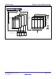
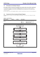
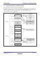
SH7670 Group Access address 31 Example of Cache Memory Setting 11 10 432 1 0 Long-word (LW) selection Tag-address comparison Entry selection Address array (ways 0 to 3) Comparison circuit Entry 0 Entry 1 · · · · · · · · · · Entry 127 LW0 LW1 LW2 LW3 16 bytes × 128 entries × 4 ways = Entry 0 V U Tag address Entry 1 · · · · · · · · · · Entry 127 Data array (ways 0 to 3) 8 KB CMP0 CMP1 CMP2 CMP3 Hit signal (Way 1) Figure 1 Overview of the Cache-Search Scheme R01AN0300EJ0101 Rev. 1.01 Oct.
SH7670 Group 2.2 Example of Cache Memory Setting Procedure for Setting the Module Used The procedure for setting up the caches is described below. Cache control register 1 (CCR1) is used to set up the cache. Program code that manipulates the cache control registers must be executed from an area for which caching is disabled. Also, access to areas for which caching has been enabled must only proceed after the CCR1 register has been read.
SH7670 Group 2.3 Example of Cache Memory Setting Description of the Sample Program In the sample program, the instruction cache and operand cache are enabled, and then data equivalent to a single cache line (16 bytes) are written to external memory (SDRAM) in write-back mode. In this case, the data are actually written to the cache and not reflected in external memory (SDRAM) until the cache entry (line) is replaced.
SH7670 Group 2.5 Example of Cache Memory Setting Allocation of Sections in the Sample Program The cache manipulation function must be placed in a cache-disabled space. In this sample program, an extended compiler function (the #pragma section directive) is used to place the function that manipulates the cache control registers (io_set_cache) in a specific section (the PCACHE section) separately from the rest of the program.
SH7670 Group 3. 3.1 Example of Cache Memory Setting Sample Program Listing Sample program list "main.c" (1) 1 /****************************************************************************** 2 * 3 * 4 * This software is supplied by Renesas Electronics Corporation and is only 5 * intended for use with Renesas products. No other uses are authorized. 6 * 7 * This software is owned by Renesas Electronics Corporation and is protected under 8 * all applicable laws, including copyright laws.
SH7670 Group 3.2 Example of Cache Memory Setting Sample program list "main.
SH7670 Group 3.3 Example of Cache Memory Setting Sample program list "main.
SH7670 Group 4. Example of Cache Memory Setting References • Software Manual SH-2A/SH2A-FPU Software Manual Rev. 3.00 The latest version of the software manual can be downloaded from the Renesas Electronics website. • Hardware Manual SH7670 Group Hardware Manual Rev. 2.00 The latest version of the hardware user's manual can be downloaded from the Renesas Electronics website. R01AN0300EJ0101 Rev. 1.01 Oct.
SH7670 Group Example of Cache Memory Setting Website and Support Renesas Electronics Website http://www.renesas.com/ Inquiries http://www.renesas.com/inquiry All trademarks and registered trademarks are the property of their respective owners. R01AN0300EJ0101 Rev. 1.01 Oct.
Revision Record Rev. 1.00 1.01 Date Oct.31.08 Oct.15.
General Precautions in the Handling of MPU/MCU Products The following usage notes are applicable to all MPU/MCU products from Renesas. For detailed usage notes on the products covered by this manual, refer to the relevant sections of the manual. If the descriptions under General Precautions in the Handling of MPU/MCU Products and in the body of the manual differ from each other, the description in the body of the manual takes precedence. 1.
Notice 1. All information included in this document is current as of the date this document is issued. Such information, however, is subject to change without any prior notice. Before purchasing or using any Renesas Electronics products listed herein, please confirm the latest product information with a Renesas Electronics sales office. Also, please pay regular and careful attention to additional and different information to be disclosed by Renesas Electronics such as that disclosed through our website.