REJ10B0166-0100 SuperH Family E10A-USB Emulator Additional Document for User’s Manual Supplementary Information on Using the SH7339 Renesas Microcomputer Development Environment System SuperH Family E10A-USB for SH7339 HS7339KCU01HE Rev.1.00 Revision Date: Dec.
Keep safety first in your circuit designs! 1. Renesas Technology Corp. puts the maximum effort into making semiconductor products better and more reliable, but there is always the possibility that trouble may occur with them. Trouble with semiconductors may lead to personal injury, fire or property damage.
Contents Section 1 Connecting the Emulator with the User System ................................1 1.1 1.2 1.3 1.4 1.5 Components of the Emulator ............................................................................................ 1 Connecting the Emulator with the User System ............................................................... 2 Installing the H-UDI Port Connector on the User System ................................................ 3 Pin Assignments of the H-UDI Port Connector ..........
ii
Section 1 Connecting the Emulator with the User System 1.1 Components of the Emulator Table 1.1 lists the components of the emulator. Table 1.1 Components of the Emulator Classification Component Hardware Appearance Quantity Emulator box 1 User system interface cable User system interface cable 1 USB cable 1 1 Remarks HS0005KCU01H: Depth: 65.0 mm, Width: 97.0 mm, Height: 20.0 mm, Mass: 72.9 g or HS0005KCU02H: Depth: 65.0 mm, Width: 97.0 mm, Height: 20.0 mm, Mass: 73.
1.2 Connecting the Emulator with the User System To connect the E10A-USB emulator (hereinafter referred to as the emulator), the H-UDI port connector must be installed on the user system to connect the user system interface cable. When designing the user system, refer to the recommended circuit between the H-UDI port connector and the MPU. In addition, read the E10A-USB emulator user's manual and hardware manual for the related device. Table 1.
1.3 Installing the H-UDI Port Connector on the User System Table 1.3 shows the recommended H-UDI port connectors for the emulator. Table 1.3 Recommended H-UDI Port Connectors Connector Type Number Manufacturer Specifications 36-pin connector DX10M-36S Hirose Electric Co., Ltd. Screw type DX10M-36SE, DX10G1M-36SE 14-pin connector 2514-6002 Lock-pin type Minnesota Mining & Manufacturing Ltd.
Pin No. Signal Input/ Output*1 1 AUDCK 2 GND 3 AUDATA0 4 GND 5 AUDATA1 6 GND 7 8 AUDATA2 9 AUDATA3 SH7339 Pin No. Output H2 Output J4 Output Output Note K2 J3 GND Output M3 Pin No.
Signal Input/ SH7339 Output*1 Pin No. 1 TCK Input J2 2 /TRST Input L2 3 TDO Output L3 4 /ASEBRKAK Output N2 5 TMS Input K3 6 TDI Input K4 7 /RESETP *2 Output F5 8 /CA *2 Output H3 9 (GND) *4 11 UVCC 10, 12, GND Pin No. *2 *2 Note User reset Output and 13 14 *3 GND Output Notes: 1. Input to or output from the user system. 2. The slash (/) means that the signal is active-low. 3.
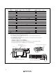
1.5 Recommended Circuit between the H-UDI Port Connector and the MPU 1.5.1 Recommended Circuit (36-Pin Type) Figure 1.3 shows a recommended circuit for connection between the H-UDI and AUD port connectors (36 pins) and the MPU when the emulator is in use. Notes: 1. Do not connect anything to the N.C. pins of the H-UDI port connector. 2. The /ASEMD0 pin must be 0 when the emulator is connected and 1 when the emulator is not connected, respectively.
12. For the AUDCK pin, guard the pattern between the H-UDI port connector and the MPU at GND level.
When the circuit is connected as shown in figure 1.3, the switches of the emulator are set as SW2 = 1 and SW3 = 1. For details, refer to section 3.8, Setting the DIP Switches, in the Debugger Part TM of the SuperH Family E10A-USB Emulator User’s Manual. VccQH = 3.0-V I/O power supply VccQ = 3.0-V/1.8-V I/O power supply All pulled-up at 4.
1.5.2 Recommended Circuit (14-Pin Type) Figure 1.4 shows a recommended circuit for connection between the H-UDI and AUD port connectors (14 pins) and the MPU when the emulator is in use. Notes: 1. Do not connect anything to the N.C. pins of the H-UDI port connector. 2. The /ASEMD0 pin must be 0 when the emulator is connected and 1 when the emulator is not connected, respectively. (1) When the emulator is used: /ASEMD0 = 0 (2) When the emulator is not used: /ASEMD0 = 1 Figure 1.
When the circuit is connected as shown in figure 1.4, the switches of the emulator are set as SW2 = 1 and SW3 = 1. For details, refer to section 3.8, Setting the DIP Switches, in the Debugger Part TM of the SuperH Family E10A-USB Emulator User’s Manual. All pulled-up at 4.7 kΩ or more VccQH VccQH VccQH VccQH VccQH VccQ VccQH = 3.0-V I/O power supply VccQ = 3.0-V/1.
Section 2 Software Specifications when Using the SH7339 2.1 Differences between the SH7339 and the Emulator 1. When the emulator system is initiated, it initializes the general registers and part of the control registers as shown in table 2.1. The initial values of the actual SH7339 registers are undefined. When the emulator is initiated from the workspace, a value to be entered is saved in a session. Table 2.
3. Low-Power States (Sleep, Software Standby, Module Standby, and U Standby) For low-power consumption, the SH7339 has sleep, software standby, module standby, and U standby states. The sleep, software standby, and module standby states are switched using the SLEEP instruction. When the emulator is used, only the sleep state can be cleared with either the normal clearing function or with the [STOP] button, and a break will occur. For the U standby state, refer to section 2.2.8, Notes on U Standby State.
8. Cache Operation during User Program Break When cache is enabled, the emulator accesses the memory by the following methods: • At memory write: Writes through the cache, then writes to the memory. • At memory read: Does not change the cache write mode that has been set. Therefore, when memory read or write is performed during user program break, the cache state will be changed. 9. Port G The AUD and H-UDI pins are multiplexed as shown in table 2.2. Table 2.
13. Memory Access during Break In the enabled MMU, when a memory is accessed and a TLB error occurs during break, it can be selected whether the TLB exception is controlled or the program jumps to the user exception handler in [TLB Mode] in the [Configuration] dialog box. When [TLB miss exception is enable] is selected, a “Communication Timeout error” will occur if the TLB exception handler does not operate correctly.
• The internal I/O registers can be accessed from the [IO] window. However, note the following when accessing the SDMR register of the bus-state controller. Before accessing the SDMR register, specify addresses to be accessed in the I/O-register definition file (SH7339.IO) and then activate the HEW. After the I/O-register definition file is created, the MPU’s specifications may be changed.
2.2 Specific Functions for the Emulator when Using the SH7339 In the SH7339, a reset must be input when the emulator is activated. Do not use the activation method described in step 12 for section 3.11 in the Debugger Part of the SuperHTM Family E10A-USB Emulator User's Manual. 2.2.1 Break Condition Functions In addition to BREAKPOINT functions, the emulator has Break Condition functions. Three types of conditions can be set under Break Condition 1, 2, 3. Table 2.
Note: When U-RAM or X/Y-RAM is accessed from the P0 space, the I-bus must be selected, and when accessed from the P2 space, the L-bus must be selected. When cache fill cycle is acquired, the I-bus must be selected. Table 2.5 lists the combinations of conditions that can be set under Break Condition 1, 2, 3. Table 2.
Table 2.7 shows the type numbers that the AUD function can be used. Table 2.7 Type Number and AUD Function Type Number AUD Function HS0005KCU01H Not supported HS0005KCU02H Supported AUD Trace Functions: This function is operational when the AUD pin of the device is connected to the emulator. Table 2.8 shows the AUD trace acquisition mode that can be set in each trace function. Table 2.
To set the AUD trace acquisition mode, click the [Trace] window with the right mouse button and select [Setting] from the pop-up menu to display the [Acquisition] dialog box. The AUD trace acquisition mode can be set in the [AUD mode1] or [AUD mode2] group box in the [Trace mode] page of the [Acquisition] dialog box. Figure 2.1 [Trace mode] Page When the AUD trace function is used, select the [AUD function] radio button in the [Trace type] group box of the [Trace mode] page.
(a) Branch Trace Function The branch source and destination addresses and their source lines are displayed. Branch trace can be acquired by selecting the [Branch trace] check box in the [AUD function] group box of the [Trace mode] page. The branch type can be selected in the [AUD Branch trace] page. Figure 2.2 [AUD Branch trace] Page (b) Window Trace Function Memory access in the specified range can be acquired by trace. Two memory ranges can be specified for channels A and B.
Figure 2.3 [Window trace] Page Notes: 1. When the [L-bus] or [I(M)-bus] radio button is selected, the bus cycles listed below will be traced. The [I-bus] and [M-bus] radio buttons are only available when the [I(M)-bus] radio button has been selected. • L-bus: A bus cycle on the L-bus generated by the CPU is acquired. A bus cycle is also acquired when the cache has been hit. • I-bus: A bus cycle on the I-bus generated by the CPU or DMA is acquired. A bus cycle is not acquired when the cache has been hit.
When U-RAM or X/Y-RAM is accessed from the P0 space, the I-bus must be selected, and when accessed from the P2 space, the L-bus must be selected. When a cache fill cycle is acquired, I-bus must be selected. 2. Address setting when X/Y-bus is selected To trace both the X/Y-bus when the X/Y-bus is accessed at the same time, the X-bus condition must be set in channel A, and the Y-bus condition must be set in channel B.
7. Do not use the AUD full-trace mode for the VIO function. 8. If a completion-type exception occurs during exception branch acquisition, the next address to the address in which an exception occurs is acquired. Internal Trace Function: This function is activated by selecting the [Internal trace] radio button in the [Trace type] group box of the [Trace mode] page. This function traces and displays the branch instructions.
4. Conditions set at Break Condition 2 are disabled when an instruction to which a BREAKPOINT has been set is executed. Do not set a BREAKPOINT to an instruction in which Break Condition 2 is satisfied. 5. When execution resumes from the address where a BREAKPOINT is specified, single-step operation is performed at the address before execution resumes. Therefore, realtime operation cannot be performed. 6.
BREAKPOINT setting, the BREAKPOINT address remains unchanged. When a BREAKPOINT is satisfied with the modified address in the VP_MAP table, the cause of termination displayed in the status bar and the [Output] window is ILLEGAL INSTRUCTION, not BREAKPOINT. 13. If an address of a BREAKPOINT cannot be correctly set in the ROM or flash memory area, a mark z will be displayed in the [BP] area of the address on the [Source] or [Disassembly] window by refreshing the [Memory] window, etc. after Go execution.
2.2.7 Performance Measurement Function The emulator supports the performance measurement function. 1. Setting the performance measurement conditions To set the performance measurement conditions, use the [Performance Analysis] dialog box and the PERFORMANCE_SET command. When any line on the [Performance Analysis] window is clicked with the right mouse button, the popup menu is displayed and the [Performance Analysis] dialog box is displayed by selecting [Setting].
Figure 2.4 [Performance Analysis] Dialog Box (b) Measurement range One of the following ranges can be specified. This depends on the item selected for [Mode] in the [Performance Analysis] dialog box. 1. From the start to the end of the user program execution (When Normal Break is selected for [Mode]) 2. From the satisfaction of the condition set in Break Condition 1 to the satisfaction of the condition set in Break Condition 2 (When Break condition 1->2 is selected for [Mode]) 3.
Notes: 1. When the second and third ranges are specified, execute the user program after the measurement start condition is set to Break Condition 1 (or Break Condition 2) and the measurement end condition to Break Condition 2 (or Break Condition 1). 2. Step operation is not possible when Break condition 1->2 or Break condition 2->1 is selected for the PERFORMANCE_SET command or in [Mode] of the [Performance Analysis] dialog box. 3.
Table 2.10 Measurement Item Selected Name Option Disabled None Elapsed time AC Number of execution states VS Branch instruction counts BT Number of execution instructions I DSP-instruction execution counts DI (Devices incorporating the DSP function can only be measured.) Instruction/data conflict cycle MAC Other conflict cycles than instruction/data OC Exception/interrupt counts EA Data-TLB miss cycle MTS (Devices incorporating the MMU function can only be measured.
Table 2.
3. Initializing the measured result To initialize the measured result, select [Initialize] from the popup menu in the [Performance Analysis] window or specify INIT with the PERFORMANCE_ANALYSIS command. 2.2.8 Notes on U Standby State Controlling Vcc (main) in the U standby state clears settings for peripheral modules in the SH7339 in which the emulator uses for debugging.
Figure 2.5 [Recovery Information] Page The following shows the procedures recovered from the U standby state. 1. In the software standby mode, when the /CA pin is asserted, the emulator enters the U standby state and the message box shown in figure 2.6 is displayed. To cancel the U standby state, be sure to end the message box before asserting /RESETP from the user system. 2. Turn Vcc (main) off. Figure 2.
3. Assert /RESETP and turn Vcc (main) on. 4. After the power has been stable, negate the /CA pin. 5. Negate /RESETP, and the U standby state is cancelled. 6. Before the program execution is restarted from the reset vector, the E10A-USB debugging function, which has been set in the [Recovery Information] page in the [Configuration] dialog box, is recovered. During this period, the HEW cannot operate. Notes: 1.
34
SuperHTM Family E10A-USB Emulator Additional Document for User's Manual Supplementary Information on Using the SH7339 Publication Date: Rev.1.00, December 24, 2004 Published by: Sales Strategic Planning Div. Renesas Technology Corp. Edited by: Technical Documentation & Information Department Renesas Kodaira Semiconductor Co., Ltd. 2004. Renesas Technology Corp., All rights reserved. Printed in Japan.
Sales Strategic Planning Div. Nippon Bldg., 2-6-2, Ohte-machi, Chiyoda-ku, Tokyo 100-0004, Japan RENESAS SALES OFFICES http://www.renesas.com Refer to "http://www.renesas.com/en/network" for the latest and detailed information. Renesas Technology America, Inc. 450 Holger Way, San Jose, CA 95134-1368, U.S.A Tel: <1> (408) 382-7500, Fax: <1> (408) 382-7501 Renesas Technology Europe Limited Dukes Meadow, Millboard Road, Bourne End, Buckinghamshire, SL8 5FH, U.K.
SuperH Family E10A-USB Emulator Additional Document for User’s Manual