REJ10J1147-0100 SuperHTM Family E10A-USB Emulator Additional Document for User’s Manual Supplementary Information on Using the SH7343 Renesas Microcomputer Development Environment System SuperHTM Family E10A-USB for SH7343 HS7343KCU01HE Rev.1.00 Revision Date: Nov.
Keep safety first in your circuit designs! 1. Renesas Technology Corp. puts the maximum effort into making semiconductor products better and more reliable, but there is always the possibility that trouble may occur with them. Trouble with semiconductors may lead to personal injury, fire or property damage.
Contents Section 1 Connecting the Emulator with the User System ................................1 1.1 1.2 1.3 1.4 1.5 Components of the Emulator ............................................................................................ 1 Connecting the Emulator with the User System ............................................................... 2 Installing the H-UDI Port Connector on the User System ................................................ 3 Pin Assignments of the H-UDI Port Connector ..........
ii
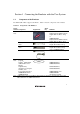
Section 1 Connecting the Emulator with the User System 1.1 Components of the Emulator The E10A-USB emulator supports the SH7343. Table 1.1 lists the components of the emulator. Table 1.1 Components of the Emulator Classification Component Hardware Appearance Quantity Emulator box 1 User system interface cable User system interface cable 1 USB cable 1 1 Remarks HS0005KCU01H: Depth: 65.0 mm, Width: 97.0 mm, Height: 20.0 mm, Mass: 72.9 g or HS0005KCU02H: Depth: 65.0 mm, Width: 97.0 mm, Height: 20.
1.2 Connecting the Emulator with the User System To connect the E10A-USB emulator (hereinafter referred to as the emulator), the H-UDI port connector must be installed on the user system to connect the user system interface cable. When designing the user system, refer to the recommended circuit between the H-UDI port connector and the MPU. In addition, read the E10A-USB emulator user's manual and hardware manual for the related device. Table 1.
1.3 Installing the H-UDI Port Connector on the User System Table 1.3 shows the recommended H-UDI port connectors for the emulator. Table 1.3 Recommended H-UDI Port Connectors Connector Type Number Manufacturer Specifications 36-pin connector DX10M-36S Hirose Electric Co., Ltd. Screw type DX10M-36SE, DX10G1M-36SE 14-pin connector 2514-6002 Lock-pin type Minnesota Mining & Manufacturing Ltd.
Pin No. Signal Input/ Output *1 1 AUDCK Output 2 GND 3 AUDATA0 4 GND 5 AUDATA1 6 GND 7 AUDATA2 8 GND 9 AUDATA3 Output Output Output Output SH7343 Pin No. Note Y13 AA14 V14 AB14 W13 Pin No.
SH7343 Pin No. Signal Input/ Output*1 1 TCK Input AB15 2 /TRST Input W14 Output Y14 Input/ AA13 Pin No. 3 *2 TDO 4 /ASEBRK / 5 6 7 *2 BRKACK output TMS Input W15 TDI Input V15 Output V16 /RESETA Output AB17 /RESETMFI Output E11 /RESETP 8 N.C. 9 (GND) 11 UVCC 10, 12, GND *2 Note User reset *5 *4 Output and 13 14 GND *3 Output Notes: 1. Input to or output from the user system. 2. The symbol (/) means that the signal is active-low. 3.
1.5 Recommended Circuit between the H-UDI Port Connector and the MPU 1.5.1 Recommended Circuit (36-Pin Type) Figure 1.3 shows a recommended circuit for connection between the H-UDI and AUD port connectors (36 pins) and the MPU when the emulator is in use. Notes: 1. Do not connect anything to the N.C. pins of the H-UDI port connector. 6 2. The MPMD pin must be 0 when the emulator is connected and 1 when the emulator is not connected, respectively.
When the circuit is connected as shown in figure 1.3, the switches of the emulator are set as SW2 TM = 1 and SW3 = 1. For details, refer to section 3.8, Setting the DIP Switches, in the SuperH Family E10A-USB Emulator User’s Manual. VccQ = 2.85-V I/O power supply All pulled-up at 4.7 kΩ or more VccQ VccQ VccQ VccQ VccQ VccQ H-UDI port connector (36-pin type) 2 4 6 8 10 12 14 16 18 20 22 24 26 28 30 32 34 36 GND AUDCK GND AUDATA0 GND AUDATA1 GND AUDATA2 GND AUDATA3 GND AUDSYNC GND N.C.
1.5.2 Recommended Circuit (14-Pin Type) Figure 1.4 shows a recommended circuit for connection between the H-UDI and AUD port connectors (14 pins) and the MPU when the emulator is in use. Notes: 1. Do not connect anything to the N.C. pins of the H-UDI port connector. 8 2. The MPMD pin must be 0 when the emulator is connected and 1 when the emulator is not connected, respectively. (1) When the emulator is used: MPMD = 0 (2) When the emulator is not used: MPMD = 1 Figures 1.
When the circuit is connected as shown in figure 1.4, the switches of the emulator are set as SW2 TM = 1 and SW3 = 1. For details, refer to section 3.8, Setting the DIP Switches, in the SuperH Family E10A-USB Emulator User’s Manual. VccQ = 2.85-V I/O power supply VccQ VccQ VccQ All pulled-up at 4.7 kΩ or more VccQ VccQ VccQ H-UDI port connector (14-pin type) TCK 9 (GND) 10 GND 12 13 GND GND 14 GND TRST TDO SH7343 1 TCK 2 TRST 3 TDO ASEBRK 4 / BRKACK 5 TMS 6 TDI RESET N.C.
10
Section 2 Software Specifications when Using the SH7343 2.1 Differences between the SH7343 and the Emulator 1. When the emulator system is initiated, it initializes the general registers and part of the control registers as shown in table 2.1. The initial values of the actual SH7343 registers are undefined. When the emulator is initiated from the workspace, a value to be entered is saved in a session. Table 2.
3. Low-Power States (Sleep, Software Standby, Module Standby, U Standby, and R Standby) For low-power consumption, the SH7343 has sleep, software standby, module standby, U standby, and R standby states. The sleep, software standby, and module standby states are switched using the SLEEP instruction. When the emulator is used, the sleep and software standby states can be cleared with either the normal clearing function or with the [STOP] button, and a break will occur.
8. Cache Operation during User Program Break When cache is enabled, the emulator accesses the memory by the following methods: • At memory write: Writes through the cache, then issues a single write to outside. The LRU is not updated. • At memory read: Reads memory from the cache. The LRU is not updated. Therefore, when memory read or write is performed during user program break, the cache state does not change. • At breakpoint set: Disables the instruction cache. 9.
12. Memory Access during Break In the enabled MMU, when a memory is accessed and a TLB error occurs during break, it can be selected whether the TLB exception is controlled or the program jumps to the user exception handler in [TLB Mode] in the [Configuration] dialog box. When [TLB miss exception is enable] is selected, a “Communication Timeout error” will occur if the TLB exception handler does not operate correctly.
• Verify In the [IO] window, the verify function of the input value is disabled. 15. Illegal Instructions If illegal instructions are executed by STEP-type commands, the emulator cannot go to the next program counter. 16. [Reset CPU] and [Reset Go] in the [Debug] Menu When a reset is issued from [Reset CPU] or [Reset Go] in the [Debug] menu, the clock pulse generator or watchdog timer is not initialized.
2.2 Specific Functions for the Emulator when Using the SH7343 2.2.1 Event Condition Functions The emulator is used to set 12 event conditions (Ch1 to Ch12) and the software trace. Table 2.4 lists the conditions of Event Condition. Table 2.4 Types of Event Conditions Event Condition Type Description Address bus condition (Address) Breaks when the SH7343 address bus value or the program counter value matches the specified value.
Table 2.
Table 2.
Sequential Setting: In the emulator, sequential setting of an Event Condition is enabled. Table 2.6 Sequential Event Conditions Type Event Condition Description [CPU 2 Channel Ch2 -> 1 Sequential Sequential Event] Page Halts a program when a condition is satisfied in the order of Event Condition 2, 1. An event condition must be set for Ch2 and Ch1. Ch4 -> 3 Halts a program when a condition is satisfied in the order of Event Condition 4, 3. An event condition must be set for Ch4 and Ch3.
Table 2.6 Sequential Event Conditions (cont) Type Event Condition Description [CPU CPU Extend Sequential Event] Page (cont) Expands the [CPU Sequential Extend] page. The sequential setting is enabled with any combination. For details, refer to section 2.2.1, Sequential Break Extension Setting, in this manual. [SystemBus SystemBus Ch9 -> 8 Sequential Sequential Event] Page Event Halts a program when a condition is satisfied for Event Condition 9, 8. An event condition must be set for Ch9 and Ch8.
Sequential Break Extension Setting: Figure 2.1 [CPU Sequential Extend] Page (a) Indicates the channel name for setting conditions. (b) Selects a condition that is satisfied before the channel which sets up conditions. When a channel name is selected, it is required that the condition of the channel selected here must have already been satisfied. When [CPU Match flag] is selected, the CPU match flag must be set. When a condition is selected by the channel selected here, no break will occur.
Usage Example of Sequential Break Extension Setting: A tutorial program provided for the product is used as an example. For the tutorial program, refer to section 6, Tutorial, in the TM SuperH Family E10A-USB Emulator User’s Manual. The conditions of Event Condition are set as follows: 1. Ch1 Breaks address H’00001068 when the condition [Prefetch address break after executing] is satisfied. 2. Ch2 Breaks address H’00001058 when the condition [Prefetch address break after executing] is satisfied. 3.
Figure 2.
2.2.2 Trace Functions The emulator supports the trace functions listed in table 2.7. Table 2.7 Trace Functions Function Internal Trace AUD Trace Memory Output Trace Branch trace Supported (eight branches) Supported Supported Range memory access trace Supported (eight events) Supported Supported Software trace Supported (eight events) Supported Supported Table 2.8 shows the type numbers that the AUD function can be used. Table 2.
Branch Trace Functions: The branch source and destination addresses, their source lines, branch types, and types of accessed bus masters are displayed. [Setting Method] Select the check box in the [Branch] group box in the [Branch trace] page of the [Branch trace] dialog box that opens by double-clicking on the Ch12 (Branch) column of the [Eventpoint] window. The branch condition to be acquired can be set. Figure 2.
Range Memory Access Trace Functions: The memory access within the specified range is acquired by a trace. The read cycle, write cycle, or read/write cycle can be selected as the bus type, ASID value, or bus cycle for trace acquisition. [Setting Method] (i) To open the [Event condition 5] or [Event condition 6] dialog box, double-click on the Ch5 (OA) or Ch6 (OA) column of the [Eventpoint] window.
(iii) Open the [ASID] page, remove the check mark of the [Don’t care] check box, and enter the ASID value to be set. When the ASID value is not set as a condition, do not remove the check mark of the [Don’t care] check box. (iv) Open the [Bus state] page and specify the bus type and bus cycle that are to be set. Figure 2.5 [Bus State] Page (v) Selecting the [Acquire trace] check box in the [Action] page enables acquiring memory access within the range.
Software Trace Function: Note: This function can be supported with SHC/C++ compiler (manufactured by Renesas Technology Corp.; including OEM and bundle products) V6.0 or later. However, SHC/C++ compiler (including OEM and bundle products) V8.0 or later is needed when instructions other than those compatible with SH4 are output. When a specific instruction is executed, the PC value at execution and the contents of one general register are acquired by trace.
AUD Trace Functions: This function is operational when the AUD pin of the device is connected to the emulator. It is activated by selecting the [AUD trace] radio button in the [Trace type] group box of the [Trace mode] page. Set the trace condition to be used. Table 2.9 shows the AUD trace acquisition mode that can be set in each trace function. Table 2.
To set the AUD trace acquisition mode, click the [Trace] window with the right mouse button and select [Setting] from the pop-up menu to display the [Acquisition] dialog box. The AUD trace acquisition mode can be set in the [Trace Mode 1] or [Trace Mode 2] group box in the [Trace Mode] page of the [Acquisition] dialog box. Figure 2.
Notes on AUD Trace: 1. When the trace display is performed during user program execution, the mnemonics, operands, or source is not displayed. 2. The AUD branch trace function outputs the differences between newly output branch source addresses and previously output branch source addresses. The window trace function outputs the differences between newly output addresses and previously output addresses. If the previously output address is the same as the upper 16 bits, the lower 16 bits are output.
Memory Output Trace Functions: This function is activated by selecting the [Use Memory trace] radio button in the [Trace type] group box of the [Trace mode] page. In this function, write the trace data in the specified user memory range. Specify the start address to output a trace for the [Start] edit box in the [User memory area] group box, and the end address for the [End Address] edit box. Set the trace condition to be used. Table 2.
To set the memory-output trace acquisition mode, click the [Trace] window with the right mouse button and select [Setting] from the pop-up menu to display the [Acquisition] dialog box. The AUD trace acquisition mode can be set in the [Trace Mode 1] or [Trace Mode 2] group box in the [Trace Mode] page of the [Acquisition] dialog box. Figure 2.
Notes: 1. The memory range for which trace is output is the address on the system bus and not supported for the MMU or cache. 2. In the memory range for output, do not specify the ranges that the user program has been downloaded or the user program accesses. 3. The range for trace output must be 1 MB or less. 2.2.3 Notes on Using the JTAG (H-UDI) Clock (TCK) and AUD Clock (AUDCK) 1. Set the JTAG clock (TCK) frequency to lower than the frequency of the SH7343 peripheral module clock (CKP). 2.
command setting is disabled. The ASID value of the SH7343 PTEH register during command input is used. When VPMAP_SET command setting is enabled, a BREAKPOINT is set to a physical address into which address translation is made according to the VP_MAP table. However, for addresses out of the range of the VP_MAP table, the address to which a BREAKPOINT is set depends on the SH7343 MMU status during command input.
2.2.5 Notes on Setting the [Event Condition] Dialog Box and the BREAKCONDITION_ SET Command 1. When [Go to cursor], [Step In], [Step Over], or [Step Out] is selected, the settings of Event Condition 3 are disabled. 2. When an Event Condition is satisfied, emulation may stop after two or more instructions have been executed. 3.
2.2.8 Performance Measurement Function The emulator supports the performance measurement function. 1. Setting the performance measurement conditions To set the performance measurement conditions, use the [Performance Analysis] dialog box and the PERFORMANCE_SET command. When a channel line on the [Performance Analysis] window is clicked with the right mouse button, the popup menu is displayed and the [Performance Analysis] dialog box is displayed by selecting [Setting]. Figure 2.
Note: For the command line syntax, refer to the online help. (a) Specifying the measurement start/end conditions Set the performance measurement conditions in the [Action] page after conditions have been set in the [Event Condition] dialog box that is opened by double-clicking Ch1 to Ch6 and Ch8 to Ch12 on the [Event Condition] sheet of the [Eventpoint] window. Notes: 1.
Figure 2.9 [Action] Page Note: PA1 or PA2 cannot be set for Ch8 and Ch9.
(b) Measurement tolerance • The measured value includes tolerance. • Tolerance will be generated before or after a break. For details, see table 2.14. (c) Measurement items Items are measured in the [Performance Analysis] dialog box for each channel from Ch1 to Ch4. A maximum of four conditions can be specified at the same time. Table 2.12 shows the measurement items. (Options in table 2.12 are parameters for of the PERFORMANCE_SET command.
Table 2.12 Measurement Items Classification Type Measurement Item Option Note None Not measured. Elapsed cycles AC Except for power-on period; counted by the CPU clock. Cycles executed in privileged mode PM The number of privilegedmode cycles among the number of elapsed cycles. Cycles for asserting the SR.BL bit BL The number of cycles when the SR.BL bit = 1 among the number of elapsed cycles.
Table 2.12 Measurement Items (cont) Classification Type Measurement Item Option Note CPU performance (cont) Stalled cycle Cycles stalled in fulltrace mode (with multi-counts) SFM All items are counted independently. Cycles stalled in fulltrace mode (without multi-counts) SF This item is not counted if the stall cycle is generated simultaneously with a stall cycle that has occurred due to instruction execution.
Table 2.12 Measurement Items (cont) Classification Type Measurement Item Option Note Instruction bus performance (cont) Instruction (cont) Number of instruction cache miss ICM The number of cache misses by an instruction cache access (the number of accesses to the outside of the CPU core due to a cache miss). Number of internalRAM access for instruction fetch (XYRAM or L memory) XL The number of accesses for the XY memory in the SH7343 during memory accesses of the opcode.
Table 2.12 Measurement Items (cont) Classification Type Measurement Item Option Note Operand bus performance (cont) Access count (cont) Number of internalRAM access for operand fetch (WRITE) (XY-RAM or L memory) XLW The number of accesses to XY memory in the SH7343 during memory access (write) of an operand. (Accesses via the XY bus and the operand bus are included. When MOVX and MOVY are executed simultaneously, it increments one count regardless of the read or write.
Table 2.12 Measurement Items (cont) Classification Type Measurement Item Option Note Operand bus performance (cont) Waited cycle Waited cycles for operand fetch (READ) WOR The number of wait cycles by a memory access (read) of an operand. Waited cycles for operand fetch (WRITE) WOW The number of wait cycles by a memory access (write) of an operand.
Table 2.13 shows the measurement items and methods that are mainly used. Table 2.
Each measurement condition is also counted when conditions in table 2.14 are generated. Table 2.14 Performance Measurement Conditions to be Counted Measurement Condition Notes No caching due to the settings of TLB cacheable bit Counted for accessing the cacheable area. Cache-on counting Accessing the non-cacheable area is counted less than the actual number of cycles and counts. Accessing the cacheable, X/Y-RAM, and U-RAM areas is counted more than the actual number of cycles and counts.
48
SuperH™ Family E10A-USB Emulator Additional Document for User's Manual Supplementary Information on Using the SH7343 Publication Date: Rev.1.00, November 2, 2005 Published by: Sales Strategic Planning Div. Renesas Technology Corp. Edited by: Customer Support Department Global Strategic Communication Div. Renesas Solutions Corp. © 2005. Renesas Technology Corp., All rights reserved. Printed in Japan.
Sales Strategic Planning Div. Nippon Bldg., 2-6-2, Ohte-machi, Chiyoda-ku, Tokyo 100-0004, Japan RENESAS SALES OFFICES http://www.renesas.com Refer to "http://www.renesas.com/en/network" for the latest and detailed information. Renesas Technology America, Inc. 450 Holger Way, San Jose, CA 95134-1368, U.S.
SuperHTM Family E10A-USB Emulator Additional Document for User’s Manual Supplementary Information on Using the SH7343