User Manual 32 Starter Kit for V850E2/FG4-L User Manual: Hardware RENESAS MCU V850E2 F-Series Y-ASK-V850E2-FG4L All information contained in these materials, including products and product specifications, represents information on the product at the time of publication and is subject to change by Renesas Electronics Corp. without notice. Please review the latest information published by Renesas Electronics Corp. through various means, including the Renesas Electronics Corp. website (http://www.renesas.
Starter Kit for V850E2/FG4-L User Manual Notice 1. All information included in this document is current as of the date this document is issued. Such information, however, is subject to change without any prior notice. Before purchasing or using any Renesas Electronics products listed herein, please confirm the latest product information with a Renesas Electronics sales office.
Starter Kit for V850E2/FG4-L User Manual Table of Contents 1. Introduction ...............................................................................................................................4 2. Quick Start – Connector and jumper overview ......................................................................5 2.1 2.2 2.3 2.4 2.5 3. Software...................................................................................................................................16 3.1 3.2 4.
Starter Kit for V850E2/FG4-L User Manual 1. Introduction The Starter Kit for V850E2/FG4-L serves as a simple and easy to use platform for evaluating the features and performance of Renesas Electronics’ 32-bit V850E2/FG4-L™ microcontrollers.
Starter Kit for V850E2/FG4-L User Manual 2.
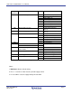
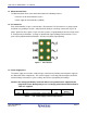
Starter Kit for V850E2/FG4-L User Manual CN3 Pin Function Pin Pin Function Pin 1 GND P11_8 2 1 GND P4_1 2 3 GND P11_9 4 3 GND P4_2 4 5 GND P10_0 6 5 GND P4_3 6 7 GND P10_1 8 7 GND P4_4 8 9 GND P10_2 10 9 GND P4_5 10 11 GND P10_3 12 11 GND P4_6 12 13 GND P10_4 14 13 GND P4_7 14 15 GND P10_5 16 15 GND P4_8 16 17 GND P10_6 18 17 GND P4_9 18 19 GND P10_7 20 19 GND P4_10 20 21 GND P10_8 22 21 GND P3_2 22 23 GND P10_9
Starter Kit for V850E2/FG4-L User Manual Jumper / Connector CN5 Description Setting Note Micro Controller power distribution 1–2 3–4 5–6 7–8 9 – 10 11 – 12 13 – 14 15 – 16 Common VDD rail (Note 2) A0VDD to µC REG1VDD to µC E1VDD to µC E0VDD to µC REG0VDD to µC OSCVDD to µC I0VDD to µC Supply by E1 Debugger (Note 3) +3.3V to +5.
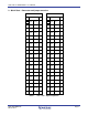
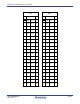
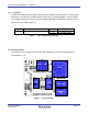
Starter Kit for V850E2/FG4-L User Manual Board Overview Figure 1 provides a top level view of the Starter Kit. Highlighted in the image are several areas of functionality. Blue: Microcontroller Area Red: Power Supply Area Green: Functional Areas These areas are described in detail in the following sections. DC IN / Power UART / LIN CAN0 CAN1 DEBUG (E1) Not used Figure 1.
Starter Kit for V850E2/FG4-L User Manual 2.1 Microcontroller Area The Microcontroller Area of the Starter Kit includes the following features: • Interfaces to all microcontroller I/O pins • Clock supply for microcontroller (16MHz) 2.2 Pin Interfaces Each microcontroller I/O pin is connected to a Pin Interface. The Pin Interface is a group of pads that allow easy probing of I/O pins, and provide the ability to selectively connect the I/O pins to power, ground or other signals.
Starter Kit for V850E2/FG4-L User Manual 2.3.1 Voltage Rail The Main Board provides two options for powering the board’s integrated circuits. Jumper CN6 is provided to select from the available voltage sources (E1 On-Chip debugger or external supply), or to completely disconnect the rail. A green indicator LED, D8, is provided to easily observe the power state of the VDD voltage rail Jumper CN6 Description Starter Kit supply voltage selection Table 5.
Starter Kit for V850E2/FG4-L User Manual 2.4.1 LEDs 2.4.1.1 White LED (High Brightness) A RGB white high brightness / high power LED, D1, is provided to allow visual observation of microcontroller output port state. The LED signal is active high. LED D1 Device Port P0_15 Table 6. White LED Signal The maximum output power of D1 can be limited by jumper CN14: Jumper CN14 Setting 1-2 3-4 open Table 7.
Starter Kit for V850E2/FG4-L User Manual 2.4.2 Pushbutton Switches Two pushbutton switches, SW1 and SW2, are provided to allow the switching of microcontroller input port states. The switches are active low and normally open. Switch SW1 SW2 Device signal RESET P0_0 (INTP0) Table 10. Active Level low low Inactive State open open Pushbutton Switch Signals 2.4.3 Analog Input - Potentiometer Potentiometer R25 is provided to generate analog voltages to the microcontroller’s analog input ADAA0I0.
Starter Kit for V850E2/FG4-L User Manual 2.4.4 Serial Communications Interfaces 2.4.4.1 RS232 and LIN One RS232 transceiver, IC20, is supplied to provide a serial interface. The transceiver is connected to the microcontroller’s UART interface (URTE10). One Local Interconnect Network transceiver, IC21, is supplied to provide a LIN interface. The transceiver is connected to the microcontroller’s LIN capable UART interface (URTE11).
Starter Kit for V850E2/FG4-L User Manual The operation modes of the LIN transceiver can be controlled by jumper CN9: Jumper CN9 Table 15. Position 1–2 3-4 Description Sleep disabled Local wake-up input (negative edge triggered) CN9 – LIN transceiver mode control Please refer to the LIN transceiver’s data sheet for details. 2.4.4.2 CAN Interfaces CAN transceivers, IC24 and IC25, are supplied to provide two CAN bus interfaces.
Starter Kit for V850E2/FG4-L User Manual Transceiver IC24 (CAN0) IC25 (CAN1) All FCAN instance FCN0 FCN1 All Table 17.
Starter Kit for V850E2/FG4-L User Manual 2.5 On-chip Debug and Flash Programming Connector Connectors CN15 is provided to allow the connection of microcontroller debug and flash programming tools. Connector CN15 is a 14 pin, 0.1” pin pitch connector. The pinout of this connector allows the connection of the Renesas E1 On-chip debugger. 3.
Starter Kit for V850E2/FG4-L User Manual Precautions 3.1 Do not look into the LED beam! Special care must be taken with the high power LED D1 and RGB LED D6! 3.2 Power supply limitation of E1 Debugger When power supply of E1 On-Chip debugger is used please note that the maximum current provided by the debugger is limited to 200mA. Thus external power supply is required in case all functions on the Starter Kit are used to full extend.
Starter Kit for V850E2/FG4-L User Manual 4.
A B C D E 1B6<> BI ZBUS<100..
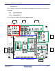
A B C D E 9 1C7<> BI 12.0V VBAT UART_LIN<1..4> 3 4 1 2 1 3 R10 10K EIA0603 1% CN9 1 3 2 4 SMD 4 23000137 8 2 4 5.0V VDD C82 100N 100N EIA0603 C85 470N C84 C2PLUS C2MINUS T1IN_TTL T2IN_TTL R1OUT_TTL R2OUT_TTL 5 6 12 11 13 10 17 16 1 RXD 2 NSLP 3 NWAKE 8 INH TXD LIN BAT GND 4 6 7 5 R1IN_RS232 R2IN_RS232 T1OUT_RS232 T2OUT_RS232 VMINUS VPLUS EN 12.
REVISION HISTORY Rev. Starter Kit for V850E2/FG4-L User Manual: Hardware Date Description Page 1.
V850E2/FG4-L Starter Kit User Manual: Hardware Publication Date: Rev.1.
http://www.renesas.com SALES OFFICES Refer to "http://www.renesas.com/" for the latest and detailed information. Renesas Electronics America Inc. 2880 Scott Boulevard Santa Clara, CA 95050-2554, U.S.A. Tel: +1-408-588-6000, Fax: +1-408-588-6130 Renesas Electronics Canada Limited 1101 Nicholson Road, Newmarket, Ontario L3Y 9C3, Canada Tel: +1-905-898-5441, Fax: +1-905-898-3220 Renesas Electronics Europe Limited Dukes Meadow, Millboard Road, Bourne End, Buckinghamshire, SL8 5FH, U.
V850E2/Fx4 Starter Kit R20UT0939ED0100