
Data Sheet
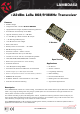

LAMBDA62 LoRa Transceiver
DS-LAMBDA62-6
Page 7
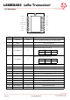
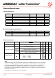
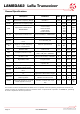
Absolute Maximums
Symbol Parameter Minimum Maximum Unit
V
dd
Positive power supply -0.3 +3.9 V
V
in
Voltage on Digital Inputs -0.3 Vdd+0.3 V
V
in
Voltage on Analogue Inputs -0.3 Vdd+0.3 V
RX Max Rx input power +10 dBm
T
op
Operating temperature -40 +85 ˚C
T
st
Storage temperature -55 115 ˚C
Symbol Parameter Minimum Maximum Unit
V
dd
Positive power supply 1.8 3.7 V
T
op
Working temperature -40 85 ˚C
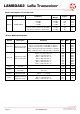
Parameter Symbol Test Min Typ Ma
x
Unit
Supply Voltage Range
V
DD
1.8 3.3 3.7
Power Saving Modes
I
Shutdown
All blocks of IC OFF.
—
160
—
nA
I
Standby
Register values maintained.
—
600
—
nA
I
Ready
Crystal Oscillator and Main Digital Regulator
ON, all other blocks OFF.
—
—
mA
TX Mode Current
RFOP = +22dBm @ 868/915MHz
RFOP = +20dBm
RFOP = +17dBm
RFOP = + 14dBm
—
118
102
95
90
mA
DC Characteristics
Electrical Specifications
Recommended Operating Conditions
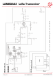
Note:
The hardware design uses the internal LDO regulator (not the SMPS DC-DC), we chose not to imple-
ment the internal BUCK regulator because in our experience, when a baery is reaching end of life
the voltage it provides starts to drop and then avalanches in a non linear curve in a short me.
It is only at this stage that the SMPS provides a benet over and above the LDO regulator, and con-
sidering the cost of the large inductor the SMPS requires its not jused for a marginal extension in
me the circuit obtains
If the SMPS is required please contact our Sales Dept