Eclipse Series RF Technology rfinfo@rftechnology.com.au May, 2005 R70/R71 and R150 Receiver Operation and Maintenance Manual This manual is produced by RF Technology Pty Ltd.
CONTENTS CONTENTS Contents 1 Operating Instructions 1.1 Front Panel Controls and Indicators 1.1.1 Mon. Volume 1.1.2 Mon. Sq. 1.1.3 N. SQ 1.1.4 C. SQ 1.1.5 Line 1.1.6 PWR LED 1.1.7 SQ LED 1.1.8 Alarm LED 4 4 4 4 5 5 5 5 5 6 2 Receiver Internal Jumper Options 2.1 JP1: 240Hz Notch Filter 2.2 JP2: Audio Response 2.3 JP3: Audio Filter In/Out 2.4 JP4: 600Ω Line dc Loop COS 2.5 JP6: COS Polarity 2.6 JP7/8/9: dc Loop COS Configuration 2.7 JP7, JP8, JP9: Direct Output COS 2.8 JP11 EPROM Type 2.
CONTENTS 7 B CONTENTS Specifications 7.1 General Description 7.1.1 Channel Capacity 7.1.2 CTCSS 7.1.3 Channel Programming 7.1.4 Channel Selection 7.1.5 Micropressor 17 17 17 17 17 18 18 7.2 Physical Configuration 18 7.3 Front Panel Controls, Indicators and Test Points 7.3.1 Controls 7.3.2 Indicators 7.3.3 Test Points 18 18 18 19 7.4 Electrical Specifications 7.4.1 Power Requirements 7.4.2 Frequency Range and Channel Spacing 7.4.3 Frequency Synthesizer Step Size 7.4.4 Frequency Stability 7.4.
1 OPERATING INSTRUCTIONS WARNING Changes or modifications not expressly approved by RF Technology could void your authority to operate this equipment. Specifications may vary from those given in this document in accordance with requirements of local authorities. RF Technology equipment is subject to continual improvement and RF Technology reserves the right to change performance and specification without further notice. 1 Operating Instructions 1.1 Front Panel Controls and Indicators 1.1.1 Mon.
1.1 OPERATING INSTRUCTIONS 1.1 Front Panel Controls and Indicators 2. Turn the N. SQ. adjustment counter clockwise until the squelch opens and noise is heard from the speaker. Adjust the VOLUME to a comfortable listening level. 3. In the absence of any on channel signal, turn the N.SQ. screw clockwise until the noise in the speaker is muted. Then turn the screw two additional turns in the clockwise direction. 1.1.4 C.SQ The C.SQ trimpot is used to set the carrier squelch sensitivity.
2 RECEIVER INTERNAL JUMPER OPTIONS The LED and squelch function are controlled by noise, carrier and tone squelch circuits. 1.1.8 ALARM LED The ALARM LED can indicate the detection of several different fault conditions by the self test circuits. The alarm indicator shows the highest priority fault present. Receivers using software issue 5 and higher use the cadence of the LED flash sequence to indicate the alarm condition. Refer to table 1.
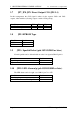
2.2 2.2 JP2: Audio Response Condition 750 uSec. de-emphasis Flat response 2.3 2 RECEIVER INTERNAL JUMPER OPTIONS JP2: Audio Response Position 1-2 * 2-3 JP3: Audio Filter In/Out JP3 bypasses the 300Hz high-pass filter and 240Hz notch filter if necessary. Condition Hi-pass, Notch In Flat response 2.4 Position 2-3 * 1-2 JP4: 600Ω Line dc Loop COS JP4 allows the dc return path through the output audio transformer to be broken, to permit dc signaling via the audio pair or wires.
2 RECEIVER INTERNAL JUMPER OPTIONS 2.7 2.7 JP7/8/9 Direct Output COS JP7, JP8, JP9: Direct Output COS (JP4 2-3) In this arrangement, the COS signal is taken via the separate COS+ and COSoutputs, either with free (floating) output or with +12Vdc pull-up. Condition +12 Vdc Direct Output Free Switch Output 2.8 JP7 2-3 1-2 JP8 OFF OFF JP9 OFF OFF JP11 EPROM Type Condition 27C256 27C64 2.
RECEIVER INTERNAL JUMPER OPTIONS 2 RX PCB TX PCB The Receiver and Transmitter modules plug into the back plane DB25/F connectors Miniature spade connectors (2.1 x 0.6 x 7mm) are captive/ soldered at the labelled points. To configure: Solder wire connections between appropriate points.
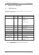
3 RECEIVER I/O CONNECTIONS 3.1 25 Pin Connector 3 Receiver I/O Connections 3.1 25 Pin Connector The D-shell 25 pin connector is the main interface to the receiver. The pin connections are described in table 3.
4 FREQUENCY PROGRAMMING 4 Frequency Programming Channel and tone frequency programming is most easily acomplished with RF Technology TecHelp/Service Monitor 2000 software. This software can be run on an IBMcompatible/Windows PC and provides a number of additional useful facillities. TecHelp/Service Monitor 2000 allows setting of the adaptive noise squelch threshold, provides a simple means of calibrating the signal strength output and minimum signal alarm.
5 CIRCUIT DESCRIPTION 5.2 IF Section A two pole 45 MHz crystal filter XF1 is used between the first and second IF amplifiers. The second IF amplifier Q4 provides additional gain of 6-10dB. A two pole crystal filter is used between Q4 and the 2nd oscillator mixer. These two crystal filters provide some adjacent channel rejection and all of the second IF image frequency rejection. U1 is a monolithic oscillator and mixer IC. It converts the 45 MHz IF signal down to 455 KHz.
5.5 Audio Signal Processing 5 CIRCUIT DESCRIPTION 1.1 GHz pre-scaler, programmable divider, reference divider and phase/frequency detector. The frequency data is entered by a serial data link from the microprocessor. The phase detector output signals of U4 are used to control two switched current sources. The output of the positive and negative sources' Q10 and Q16, produce the tuning voltage which is smoothed by the loop filter components to bias the VCO varactor diode D4. 5.
5 CIRCUIT DESCRIPTION 5.8 External Squelch system connector. The filtered output can be used for re-transmission of CTCSS or DCS. The CTCSS decoder module is a micro-controller base hybrid module. Under control of the main microprocessor U15 it can decode all 38 EIA tones and 12 additional commonly used tones. The decode bandwidth is set to 1% but may be changed to 2% by a jumper on the printed circuit board. 5.
5.11 Voltage Regulator 5.11 5 CIRCUIT DESCRIPTION Voltage Regulator The dc input voltage is regulated down to 9.4 Vdc by a discrete regulator circuit. The series pass transistor Q20 is driven by error amplifiers Q21 and Q22. Q23 is used to start up the regulator and once the circuit turns on, it plays no further part in the operation. This circuit is short circuit and overload protected.
6 ALIGNMENT PROCEDURE Step 1 2 3 6.3 Step 1 2 3 4 5 6 7 Page 16 Input Select alignment frequency channel Signal generator on centre frequency channel to J1. Modulation off. As Above 6.3 IF Alignment Measure dc Volts on test socket pin 9 to pin 1 dc Volts on test socket pin 7 to pin 1 Adjust L34 to read 4.00Vdc As Above L29, L31, L36, L38 for maximum reading. Reduce generator output to keep below 2 Vdc Input Signal generator on center frequency channel to J1.
6.4 Step 1 6.5 Step 1 Line Level Adjustment Input Signal generator on centre frequency channel to J1. Modulation ON. Level 1 millivolt Measure Audio level test socket pin 6 to pin 1 Adjust RV3 for 390 mV rms Reference Oscillator Calibration Input None required Measure Frequency junction of R69 and R26 on the top of the PCB. (LO input to the mixer) 7 Specifications 7.1 General Description Adjust C181 or XO1 for L.O. +/-100 Hz L.O.
7 SPECIFICATIONS 7.1.4 7.1.4 Channel Selection Channel Selection Channel selection is by eight channel select lines. These are available through the rear panel connector. A BCD active high code applied to the lines selects the required channel. This can be supplied by pre-wiring the rack connector so that each rack position is dedicated to a fixed channel. BCD switches inside the receiver can be used to pre-set any desired channel. These eliminate the need to externally select the channel. 7.1.
7 SPECIFICATIONS 7.3.3 Test Points 7.3.3 Test Points (DB9 Connector) Line Output Level Pin 6 + Gnd (pin 1) Receive Signal Strength Pin 7 + Gnd (pin 1) Tuning Voltage Pin 9 + Gnd (pin 1) Serial Data (RS232) Pins 2/3 + Gnd (pin 1) 7.4 Electrical Specifications 7.4.1 Power Requirements Operating Voltage - 10.5 to 16 Vdc Current Drain - 250mA Max. Polarity - Negative Ground 7.4.2 Frequency Range and Channel Spacing Frequency 66 - 84 MHz 70 - 88 MHz 136 - 156 MHz 148 - 168 MHz 154 - 174 MHz 7.
7 SPECIFICATIONS 7.4.6 7.4.6 IF Frequencies IF Frequencies First IF frequency 45 MHz Second IF frequency 455 KHz 7.4.7 Sensitivity -119 dBm Max. for 12 dB SINAD -116 dBm Max. for 20 dB Quieting 7.4.8 Selectivity 25 KHz spacing - 80dB per RS204C 12 KHz spacing - 70dB per ECR-235 7.4.9 Spurious and Image Rejection 90dB 7.4.10 Inter-modulation 80dB 7.4.11 Modulation Acceptance BW 25 KHz spacing - 7.5 KHz per RS204C 12.5 KHz spacing - 3.75 KHz per RS204C 7.4.
7.4.13 Carrier Level Squelch 7.4.13 7 SPECIFICATIONS Carrier Level Squelch Carrier level squelch can be used when it is necessary to set the opening point above 26dB SINAD as may be required in link applications. The minimum adjustment range is 1 to 200µV. 7.4.14 Receiver Frequency Spread Less than 1 dB change in sensitivity over the band 7.4.15 Receiver Conducted Spurious Emissions Less than -57dBm from 1 to 2900 MHz 7.4.
7 SPECIFICATIONS 7.4.19 7.4.20 Carrier Operated Switch Output Channel Select Input/Output Coding: 8 lines BCD coded 00-99 Logic Input Levels: 0 = <0.4 Volts 1 = >3.5 Volts Internal 10K pull down resistors selects Channel 00 when all inputs are O/C. 7.4.20 Carrier Operated Switch Output Floating Opto-Coupler Output: The carrier operated switch output is via an opto-coupler. Collector and emitter connections are available to allow connection for source or sink.
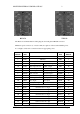
7 SPECIFICATIONS 7.4.21 CTCSS Frequency No Tone EIA Number 67.0 69.4 71.9 74.4 77.0 79.7 82.5 85.4 88.5 91.5 94.8 97.4 100.0 103.5 107.2 110.9 114.8 118.8 123.0 127.3 131.8 136.5 141.3 146.2 151.4 156.7 159.8 162.2 165.5 167.9 171.3 173.8 177.3 179.9 183.5 186.2 189.9 192.8 196.6 199.5 203.5 206.5 210.7 218.1 225.7 229.1 233.6 241.8 250.3 254.
7 SPECIFICATIONS 7.4.22 7.4.22 External Squelch Input External Squelch Input An external input is provided to squelch or mute the receiver audio output. This may be used in conjunction with an external decoder or to mute the receiver during transmissions. External Squelch Input can be connected to the T/R Relay pin on Eclipse transmitters to mute the receiver during transmission. 7.5 Connectors 7.5.1 Antenna Connector Type N Female Mounted on the module rear panel 7.5.
IN OUT +12 Vdc Direct Output Free Switch Output JP7, JP8, JP9 - Direct Output COS (JP4 2-3) Source +l2Vdc Loop Free Switch Output JP7, JP8, JP9 - dc Loop COS Configuration (JP4 1-2) Active on Signal Active on No Signal JP6 - COS Polarity dc Loop Configured by JP7, JP8, JP9 dc Loop Not Used JP4 - 600 Ohm Line dc Loop COS Hi-pass & Notch In Flat Response JP3 - Audio Filter in/Out 750 uSec.