Eclipse Series RF Technology rfinfo@rftechnology.com.
CONTENTS CONTENT Contents 1 Operating Instructions 1.1 Front Panel Controls and Indicators 1.1.1 PTT 1.1.2 Line 1.1.3 PWR LED 1.1.4 TX LED 1.1.5 ALARM LED 1.1.6 ALC LED 1.1.7 REF LED 1.1.8 TEST MIC 5 5 5 5 6 6 6 6 6 7 2 Transmitter Internal Jumper Options 2.1 JP2: EPROM type 2.2 JP3: Dc Loop PTT 2.3 JP4: Audio Input Source 2.4 JP5: 600? Termination 2.5 JP6: Input Level Attenuation 2.6 JP7: Audio Response 2.7 JP8: Sub-audible Tone source 2.8 JP9/10/11: dc Loop Configuration 2.
CONTENTS 6.3 6.4 6.5 6.6 6.7 6.8 7 TCXO Calibration Modulation Balance Tone Deviation Deviation Line Input Level Output Power CONTENTS 17 17 18 18 18 19 Specifications 7.1 Overall Descri ption 7.1.1 Channel Capacity 7.1.2 CTCSS 7.1.3 Channel Programming 7.1.4 Channel Selection 7.1.5 Micro-processor 19 19 19 19 20 20 20 7.2 Physical Configuration 20 7.3 Front Panel Controls, Indicators and Test Points 7.3.1 Controls 7.3.2 Indicators 7.3.3 Test Points 20 20 20 20 7.4 Electrical Specifications 7.4.
CONTENTS CONTENTS A Engineering Diagrams A.1 Block Diagram A.2 Circuit Diagrams A.
1 OPERATING INSTRUCTIONS WARNING Changes or modifications not expressly approved by RF Technology could void your authority to operate this equipment. Specifications may va ry from those given in this document in accordance with requirements of local authorities. RF Technology equipment is subject to continual improvement and RF Technology reserves the right to change performance and specification without further notice. 1 Operating Instructions 1.1 Front Panel Controls and Indicators 1.1.
1 OPERATING INSTRUCTIONS 1.1.
2 TRANSMITTER INTERNAL JUMPER OPTIONS 1.1.8 TEST MIC The TEST MIC. DIN socket is provided for use with a standard mobile or handset 200 Ohm dynamic microphone. The external audio inputs are disabled when the TEST MIC’S PTT is on. 2 Transmitter Internal Jumper Options In the following subsections an asterisk (*) signifies the standard (Ex-Factory) configuration of a jumper. 2.1 JP2: EPROM Type Condition 27C256 27C64 Position 2-3 * 1-2 2.
2.5 JP6: Input Level Attenuation 2.5 2 TRANSMITTER INTERNAL JUMPER OPTIONS JP6: Input Level Attenuation This jumper permits coarse input sensitivity to be set. In the default position, the unit expects a line level of 0dBm (nominal) at its Line Input. In the alternate position, levels of +20dBm (nominal) can be accepted. Condition 0dB attenuation 20dB attenuation 2.6 Position 1-2 * 2-3 JP7: Audio Response Condition 750 uSec. pre-emphasis Flat response 2.
2 TRANSMITTER INTERNAL JUMPER OPTIONS 2.10 JP17: Bypass Low Pass Filter Condition Normal Tone Input Direct Tone Input Position 1-2* 2-3 2.10 JP17: Bypass Low Pass Filter (pcb 30/9103/0009 or later) Some trunking controllers have digital encoding schemes that require the low pass filter in the tone input section to be bypassed. JP17 allows this. Normally JP17 is open circuit. Placing a link across it will bypass the low pass filter.
3 TRANSMITTER I/O CONNECTIONS Condition N DMTX board DMTX board connected 3 3.1 Position 1-2, 5-6* 2-3, 4-5 Transmitter I/O Connections 25 Pin Connector The D-shell 25 pin connector is the main interface to the transmitter. The pin connections are described in table 3.
3 TRANSMITTER I/O CONNECTIONS 3.2 Rear Panel Connectors Fig 1 RX PCB Fig 2 TX PCB The Receiver and Transmitter modules plug into the back plane DB25/F connectors To configure: Solder wire connections between appropriate points.
4 CHANNEL AND TONE FREQUENCY PROGRAMMING 4 Channel and Tone Frequency Programming Channel and tone frequency programming is most easily accomplished with RF Technology TecHelp software or the Service Monitor 2000 software. This software can be run on an IBM compatible PC and provides a number of additional useful facilities. DOS and 32-bit versions are available.
5 CIRCUIT DESCRIPTION 5.3 Power Amplifier pre-scaler, programmable divider, reference divider and phase/frequency detector. The frequency data for U6 is supplied through serial data link by the microprocessor. The phase detector output signals of U6 are used to control two switched current sources. The output of the positive and negative sources (Q3 and Q6) produces the tuning voltage which is smoothed by the loop filter components to bias the VCO varactor diode D3. 5.
5.7 Local Microphone Input 5 CIRCUIT DESCRIPTION The bridge configuration allows audio signal inversion by interchanging the positive and negative inputs and minimizes ground loop problems. Both inputs should be connected, with one lead going to the source output pin and the other connected to the source audio ground. 5.7 Local Microphone Input The local microphone input is provided for use with a standard low impedance dynamic microphone.
5 CIRCUIT DESCRIPTION 5.10 PTT & DC Remote Control When a DMTX board option is required, jumper JP23 allows the audio paths to be rerouted. The DMTX board provides for an external digital modulation input signal. When the two links on JP23 are positioned in the middle of the 6 pin header, the audio from the exciter is passed to the DMTX board via pin5 of JP5, where the signal is conditioned and then returned from the DMTX board via pin 2 of JP15, and passed to the two modulation points.
5.12 Voltage Regulator 5 CIRCUIT DESCRIPTION The analogue to digital converter is used to measure the forward and reverse power, tuning voltage and dc supply voltage. If the processor detects that the PTT_WIRE_OR signal is asserted low, it will attempt to key the exciter up. It will first attempt to key the VCO through Q10, and if the LD pin goes high, it will switch the 9.2 Volt transmit line through Q14 and Q16.
6 FIELD ALIGNMENT PROCEDURE 6.1 6.1 Standard Test Condition Standard Test Condition The following equipment and conditions are assumed unless stated otherwise: • AF signal generator with 600Ω impedance, 150-3000Hz frequency range, with level set to 387mV RMS. • Power supply set to 13.8Vdc, with a current capable of >5A. • RF 50Ω load, 30W rated, return loss <-20dB. • Jumpers set to factory default positions. 6.2 VCO Alignment 1.
6.5 Tone Deviation 6 FIELD ALIGNMENT PROCEDURE 6. Set the audio input to 150Hz, 0dBm 7. Measure deviation and adjust RV4 (line level) for a deviation of 5kHz (2.5kHz for narrow band transmitters). 8. Set the audio input to 1.5kHz, 0dBm. 9. Adjust RV2 (Mod. Bal.) for a deviation of 5kHz (2.5kHz for narrow band transmitters) 10. Repeat steps 6-9 until balance is achieved. 11. Key the transmitter off. 12. Return JP7 to its correct setting. 13. Carry out the Deviation (section 6.
6 FIELD ALIGNMENT PROCEDURES 6.8 Output Power 2. Key the transmitter on. 3. Adjust RV4 (line level) for 60% of system deviation (3kHz or 1.5kHz for narrow band systems). 4. If the test signal is varying, RV4 may be adjusted to produce a level of 234mV RMS or 660mVp-p at the audio voltage test connector pin 6 to pin 1. 5. Key the transmitter off. 6.8 Output Power 1. No audio input is required 2. Key the transmitter on. 3.
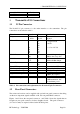
7.1.3 Channel Programming 7.1.3 7 SPECIFICATIONS Channel Programming The channel information is stored in non-volatile memory and can be programmed via the front panel test connector using a PC and RF Technology software. 7.1.4 Channel Selection Channel selection is by eight channel select lines. These are available through the rear panel connector. Internal presetting is also possible. The default (open-circuit) state is to select channel 00.
7 SPECIFICATIONS 7.3.3 7.4 Electrical Specifications Test Points Line Input – Pin 6 + Ground (pin 1) Forward Power – Pin 8 + Ground (pin 1) Reverse Power – Pin 4 + Ground (pin 1) Tuning Voltage – Pin 9 + Ground (pin 1) Serial Data (RS-232) – Pins 2 / 3 + Ground (pin 1) 7.4 7.4.1 Electrical Specifications Power Requirements Operating Voltage - 10.5 to 16 Vdc with output power reduced below 12 Vdc Current Drain - 5A Maximum, typically 0.25A Standby Polarity - Negative Ground 7.4.
7.4.8 Transmit Duty Cycle 7.4.7 7 SPECIFICATIONS Output power Preset for 2-15 or 2-25W depending upon model 7.4.8 Transmit Duty Cycle 100% to 40C, de-rating to zero at 60C. 100% to 5000ft altitude, de-rating to zero at 15,000ft. 7.4.9 Spurious and Harmonics Less than 0.25µW 7.4.10 Carrier and Modulation Attack Time Less than 20ms. Certain models have RF envelope attack and decay times controlled in the range 200µs< t r/f <2ms according to regulatory requirements. 7.4.
7 SPECIFICATIONS 7.4.18 External ALC Input 7.4.17 External Tone Input Compatible with R500 tone output 7.4.18 External ALC Input Output will be reduced 20dB by pulling the input down to below 1V. (Typically more than 40dB attenuation is available.) The input impedance is ≅10kΩ, internally pulled up to rail. The external ALC input can be connected to the power control circuit in Eclipse external power amplifiers. 7.4.
7.2.24 CTCSS 7 SPECIFICATIONS in increments of one minute. The timer is automatically reset when the PTT input is released. ____________________________________ 3 The reverse phase burst is usually sufficient to eliminate squelch tail noise in higher-quality mobiles 7.4.24 CTCSS CTCSS tones can be provided by an internal encoder or by an external source connected to the external tone input. The internal CTCSS encoding is provided by a subassembly PCB module.
. 7 SPECIFICATIONS Frequency No Tone 67.0 69.4 71.9 74.4 77.0 79.7 82.5 85.4 88.5 91.5 94.8 97.4 100.0 103.5 107.2 110.9 114.8 118.8 123.0 127.3 131.8 136.5 141.3 146.2 151.4 156.7 159.8 162.2 165.5 167.9 171.3 173.8 177.3 179.9 183.5 186.2 189.9 192.8 196.6 199.5 203.5 206.5 210.7 218.1 225.7 229.1 233.6 241.8 250.3 254.
A A ENGINEERING DIAGRAMS Engineering Diagrams Most Eclipse transmitter modules contain two PCBs, a motherboard with the control and signal generation circuitry (the exciter board), and an RF Power Amplifier board. Certain models are equipped with optional functions on piggyback PCBs atop the exciter motherboard. The exciter PCB typically has a few components whose values vary from model to model depending upon operating frequency and local regulatory constraints.
A 1 Hi-Z INPUT LINE IN U9A T1 ISO1 DIODE D10 A/D ASYNC. DATA I/O 2 MICROPROCESSOR CONTROLER U1-U5,U11,U13 250Hz LOOP FILTER SW SPDT JP4 TEST KEY 3 U10B U10A D12 TX MA5 U10C CTCSS MODULE TEST MIC. AMP. U9B H1 +9.2 Vdc TRANSMIT SUPPLY Q14,Q16 RV2 MOD.BAL. MA4 BUFFER AMPLIFIER 3 EXT.TONE INPUT INPUT AMP. U9D LINE LEVEL RV4 D1 ALM TONE DATA TX ENABLE TEST MIC. Q10 V.C.O. Q19,Q20 VCO ISOLATION AMPS MA3 Q2-Q7,Q11,Q21 MA2 2 PTT LINE IN PTT IN Tx DATA Rx DATA +13.
750 uSec.