Eclipse Series RF Technology rfinfo@rftechnology.com.
CONTENTS CONTENTS Contents 1 Operating Instructions 1.1 Front Panel Controls and Indicators 1.1.1 Mon. Volume 1.1.2 Mon. Sq. 1.1.3 N. SQ 1.1.4 C. SQ 1.1.5 Line 1.1.6 Power LED 1.1.7 SQ LED 1.1.8 Alarm LED 5 5 5 5 5 6 6 6 6 6 2 Receiver Internal Jumper Options 2.1 JP1: 240Hz Notch Filter 2.2 JP2: Audio Response 2.3 JP3: Audio Filter In/Out 2.4 JP4: 600Ω Line dc Loop COS 2.5 JP6: COS Polarity 2.6 JP7, JP8, JP9: dc Loop COS Configuration 2.7 JP7, JP8, JP9: Direct Output COS 2.8 JP11 EPROM Type 2.
CONTENTS CONTENTS 7 Specifications 7.1 General Description 7.1.1 Channel Capacity 7.1.2 CTCSS 7.1.3 Channel Programming 7.1.4 Channel Selection 7.1.5 Microprocessor 7.2 Physical Configuration 7.3 Front Panel Controls, Indicators and Test Points 7.3.1 Controls 7.3.2 Indicators 7.3.3 Test Points 7.4 Electrical Specifications 7.4.1 Power Requirements 7.4.2 Frequency Range and channel Spacing 7.4.3 Frequency Synthesizer Step Size 7.4.4 Frequency Stability 7.4.5 Nominal Antenna Impedance 7.4.
1 OPERATING INSTRUCTIONS WARNING Changes or modifications not expressly approved by RF Technology could void your authority to operate this equipment. Specifications may vary from those given in this document in accordance with requirements of local authorities. RF Technology equipment is subject to continual improvement and RF Technology reserves the right to change performance and specification without further notice. 1 Operating Instructions 1.1 Front Panel Controls and Indicators 1.1.1 Mon.
1.1 Front Panel Controls and Indicators 1.1.4 1 OPERATING INSTRUCTIONS C.SQ The C.SQ trimpot is used to set the carrier squelch sensitivity. Carrier squelch is useful at higher signal levels than those at which noise squelch can be used – typically from 1-200µ V input. It is provided mainly for use in fixed link applications where a high minimum signal to noise ratio is required or where very fast squelch operation is required for data transmission.
2 RECEIVER INTERNAL JUMPER OPTIONS issue 4 and lower use the LED flash rate to indicate the alarm condition. Refer to table 2.
2.3 2.3 2 RECEIVER INTERNAL JUMPER OPTIONS JP3: Audio Filter In/Out JP3: Audio Filter In/Out JP3 bypasses the 300Hz high-pass filter and 240Hz notch filter if necessary. Condition Hi-pass, Notch In Flat response 2.4 Position 2-3 * 1-2 JP4: 600Ω Line dc Loop COS JP4 allows the dc return path through the output audio transformer to be broken, to permit dc signaling via the audio pair of wires. Condition dc Loop Configured by JP7/8/9 dc Loop Not used 2.
4 FREQUENCY PROGRAMMING 2.8 JP11: EPROM Type Condition 27C256 27C64 2.9 Position 2-3 * 1-2 JP13: Squelch Defeat (pcb 30/9131/0004 or later) Normal squelch can be defeated with an active low signal at DB-25 pin 19. Condition Squelch operation normal Squelch Defeat 2.
4 FREQUENCY PROGRAMMING Function DC Power Channe l Select RS232 Data 600Ω Line Output Signal +12 Vdc 0 Vdc 1 2 4 8 10 20 40 80 In Out LineLine+ 150Ω / Hybrid Discriminator Audio Direct Audio Output Audio Ground Sub-Audible Audio Out Carrier Operated Sw Carrier Operated Sw External Squelch COS+ COSInput Pins 1, 14 13, 25 21 9 22 10 23 11 24 12 15 2 20 6 7 19 18 17 5 4 Specification +11.
5 CIRCUIT DESCRIPTION 5 Circuit Description 5.1 RF Section The following descriptions should be read as an aid to understanding the block and schematic diagrams at the rear of this manual. 5.1 RF Section A two section helical filter FL1 is used to limit the RF band width prior to the RF amplifier transistor Q1. The output impedance of FL1 is matched to the input of Q1 by C165, C1 and a microstrip line on the printed circuit board. Q1 is a very low noise device with good intermodulation performance.
5.3 VCO Section 5 CIRCUIT DESCRIPTION CF1 and its termination resistors R15 and R24 are the only component differences in the two versions. The limiter/discriminator IC U3 further amplifies the signal and passes it through CF2. CF2 does not contribute to the adjacent channel rejection but is used to reduce the wide band noise input to the limiter section of U3. The limiter section of U3 drives the quadrature detector discriminator.
5 CIRCUIT DESCRIPTION 5.5 5.5 Audio Signal Processing Audio Signal Processing A 4 kHz low pass filter (U27b) is used to remove high frequency noise from the signal. A 300 Hz high pass filter (U26a,b) the n removes the sub-audible tones. A 240 Hz notch filter (U26c,d) is used to improve the rejection of tones above 200 Hz. The audio can be set for either 750 uS de-emphasis or a flat response by JP2. JP2 selects the feedback network of amplifier U27c.
5.8 Microprocessor Controller 5.8 5 CIRCUIT DESCRIPTION Microprocessor Controller The microprocessor controller circuit uses an advanced eight bit processor and several support chips. The processor U15 includes EE memory for channel frequencies, tones, and other information. It also acts as an asynchronous serial port, a synchronous serial port and an analogue to digital converter. The program is stored in U12, a CMOS EPROM. U13 is an address latch for the low order address bits.
6 ALIGNMENT PROCEDURE 6.1 Standard Input Sig nal TCXO calibration may be required periodically due to crystal aging. The aging should be less than 1 ppm/year. 6.1 Standard Input Signal RF Signal Generator, 50Ω output impedance, Frequency range 350-520MHz, FM modulation at 1kHz, deviation 1.5kHz peak for 12.5KHz channel spacing, 3.0kHz peak for 25kHz channel spacing. 6.2 RF Alignment 1. Select center frequency channel. Measure dc Volts on test socket pin 9 to pin 1. Adjust C61 to read 4.25 to 4.
6.4 Line Level Adjustment 7. 6.4 1. 6.5 6 ALIGNMENT PROCEDURE Set generator level to 0.25µV, and measure SINAD on test socket pins 6 and 1. Reduce generator level to obtain 12dB SINAD. Carefully adjust L5,L6,L7,L8 to obtain the best SINAD. Reduce the generator output to maintain 12dB SINAD. Line Level Adjustment Set generator level at 1000µV (1mV), modulation on, tuned to the center frequency channel frequency, apply signal to J1. Measure the audio level on pin 6 of the test socket wrt pin 1.
7 SPECIFICATIONS 7.1.3 7.1 General Description Channel Programming The channeling information is stored in a non-volatile memory chip and can be programmed via the front panel test connector using a PC and RF Technology supplied TecHelp software. 7.1.4 Channel Selection Channel selection is by eight channel select lines. These are available through the rear panel connector. A BCD active high code applied to the lines selects the required channel.
7.2 7.3.2 7 SPECIFICATIONS Physical Configuration Indicators Power ON - Green LED Squelch Open - Yellow LED Fault Indicator - Flashing Red LED 7.3.3 Test Points Line Output Level – Pin 6 + Gnd (pin 1). Receive Signal Strength – Pin 7 + Gnd (pin 1). Tuning Voltage – Pin 9 + Gnd (pin 1). Serial Data (RS232) – Pins 2/3 + Gnd (pin 1). 7.4 Electrical Specifications 7.4.1 Power Requirements Operating Voltage - 10.5 to 16 Vdc Current Drain - 450mA Max. Polarity - Negative Ground 7.4.
7 SPECIFICATIONS 7.4.3 7.4 Electrical Specification Frequency Synthesizer Step Size 12.5 kHz 7.4.4 Frequency Stability ±1 ppm over 0 to +60 C, Standard 7.4.5 Nominal Antenna Impedance 50Ω 7.4.6 IF Frequencies First IF frequency 45 MHz Second IF frequency 455 kHz 7.4.7 Sensitivity 0.25µV (-119dBm) for 12dB SINAD 0.28µV (-118dBm) for 20dB Quieting 7.4.8 Selectivity 25 kHz spacing - 80dB per RS204C 12 kHz spacing - 70dB per ECR-235 7.4.9 Spurious and Image Rejection 90dB 7.4.
7 SPECIFICATIONS 7.4.11 Modulation Acceptance BW 7.4.11 Modulation Acceptance BW 25 kHz spacing - 7.5 kHz per RS204C 12.5 kHz spacing - 3.75 kHz per RS204C 7.4.12 Noise Squelch Adjustment Range: 6 - 26dB SINAD Minimum Attack Time: Release Time: threshold 20 ms above 20dB Quieting 150~ms at 20dB Quieting decreasing to 20ms above 2µV preset Hysteresis: Hysteresis is equal to approximately 2dB change in noise quieting 7.4.
7 SPECIFICATIONS 7.4.18 Audio Distortion Monitor Loudspeaker: 3 Watts with external speaker, 0.3 Watt with internal speaker Discriminator and Sub-Audio: Nominally equal to 1 volt peak at rated system deviation 7.4.18 Audio Distortion 750µs De-Emphasis: Less than 3% at 1 kHz and 60% of rated system deviation Flat Response: Less than 10% at 1 kHz and 60% of rated system deviation 7.4.19 Channel Select Input / Output Coding : 8 lines BCD coded 00-99 Logic Input Levels: 0 <= 1.0 Volts 1 >= 3.
7 SPECIFICATIONS Frequency No Tone EIA Number 67.0 69.4 71.9 74.4 77.0 79.7 82.5 85.4 88.5 91.5 94.8 97.4 100.0 103.5 107.2 110.9 114.8 118.8 123.0 127.3 131.8 136.5 141.3 146.2 151.4 156.7 159.8 162.2 165.5 167.9 171.3 173.8 177.3 179.9 183.5 186.2 189.9 192.8 196.6 199.5 203.5 206.5 210.7 218.1 225.7 229.1 233.6 241.8 250.3 254.
A ENGINEERING DIAGRAMS 7.4.22 7.5 Connectors External Squelch Input An external input is provided to squelch or mute the receiver audio output. This may be used in conjunction with an external decoder or to mute the receiver during transmissions. External Squelch Input can be connected to the T/R Relay pin on Eclipse transmitters to mute the receiver during transmission. 7.5 Connectors 7.5.1 Antenna Connector Type N Female Mounted on the module rear panel 7.5.
A B C D Flo Fx 1 Tx DATA Rx DATA +13.8 CARRIER SQ. TUNE V. RSSI MA1 VCO Q6,Q7 Q10-Q16 MA4 Q5 PLL IC 12.5/10 KHz STEPS U4 A/D 2 ASYNC. DATA I/O 600 MHz C45,C46,L13 4 RESONATOR HELICAL FILTER FL2, FL3 MICROPROCESSOR CONTROLER U7,U11-U16 ALM 2 +15 dBm LO OUTPUT RF AMP. Q1 250Hz LOOP FILTER VCO ISOLATION AMPS MA3 MA2 LO AMPLIFIER 2 RESONATOR HELICAL FILTER FL1 BCD CHANNEL CODE EXT. SQ. * BNC 1 LOCK DETECT DATA 12.8 MHz MX1 Q2,Q3 1st IF AMP.
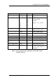
IN OUT +12 Vdc Direct Output Free Switch Output JP7, JP8, JP9 - Direct Output COS (JP4 2-3) Source +l2Vdc Loop Free Switch Output JP7, JP8, JP9 - dc Loop COS Configuration (JP4 1-2) Active on Signal Active on No Signal JP6 - COS Polarity dc Loop Configured by JP7, JP8, JP9 dc Loop Not Used JP4 - 600 Ohm Line dc Loop COS Hi-pass & Notch In Flat Response JP3 - Audio Filter in/Out 750 uSec.