Eclipse Series RF Technology rfinfo@rftechnology.com.
CONTENTS CONTENTS Contents 1 Operating Instructions 1.1 Front Panel Controls and Indicators 1.1.1 PTT 1.1.2 Line 1.1.3 PWR LED 1.1.4 TX LED 1.1.5 ALARM LED 1.1.6 ALC LED 1.1.7 REF LED 1.1.8 TEST MIC 4 4 4 4 4 4 5 5 5 5 2 Transmitter Internal Jumper Options 2.1 JP2: EPROM type 2.2 JP3: Dc Loop PTT 2.3 JP4: Audio Input Source 2.4 JP5: 600 ? Termination 2.5 JP6: Input Level Attenuation 2.6 JP7: Audio Response 2.7 JP8: Sub-audible Tone source 2.8 JP9/10/11: dc Loop Configuration 2.
CONTENTS 6.5 Tone Deviation 6.6 Deviation 6.7 Line Input Level 6.8 Output Power 7 B CONTENTS 19 19 19 19 Specifications 7.1 Overall Description 7.1.1 Channel Capacity 7.1.2 CTCSS 7.1.3 Channel Programming 7.1.4 Channel Selection 7.1.5 Micro-processor 20 20 20 20 20 20 21 7.2 Physical Configuration 21 7.3 Front Panel Controls, Indicators and Test Points 7.3.1 Controls 7.3.2 Indicators 7.3.3 Test Points 21 21 21 21 7.4 Electrical Specifications 7.4.1 Power Requirements 7.4.
1 OPERATING INSTRUCTIONS WARNING Changes or modifications not expressly approved by RF Technology could void your authority to operate this equipment. Specifications may vary from those given in this document in accordance with requirements of local authorities. RF Technology equipment is subject to continual improvement and RF Technology reserves the right to change performance and specification without further notice. 1 Operating Instructions 1.1 Front Panel Controls and Indicators 1.1.
1 OPERATING INSTRUCTIONS. 1.1.5 1.1.5 Alarm LED ALARM LED The Alarm LED can indicate several fault conditions if they are detected by the self test program. The alarm indicator shows the highest priority fault present. Transmitters using software issue 5 and higher use the cadence of the LED flash sequence to indicate the alarm condition. Refer to table 1. Transmitter using software issue 4 and lower use the LED flash rate to indicate the alarm condition. Refer to table 2.
2 TRANSMITTER INTERNAL JUMPER OPTIONS 2.1 JP2: Eprom Type 2 Transmitter Internal Jumper Options In the following subsections an asterisk (*) signifies the standard (Ex-Factory) configuration of a jumper. 2.1 JP2: EPROM Type Condition 27C256 27C64 Position 2-3 * 1-2 2.2 JP3: 600 Ohm Line Dc Loop PTT Input By default, Eclipse exciters can be keyed up by pulling the PTT signal low, or by dc loop signaling on the audio pair. This jumper enables, or disables this second method.
2 TRANSMITTER INTERNAL JUMPER OPTIONS 2.5 2.5 JP6: Input Level Attenuation JP6: Input Level Attenuation This jumper permits coarse input sensitivity to be set. In the default position, the unit expects a line level of 0dBm (nominal) at its Line Input. In the alternate position, levels of +20BdBm (nominal) can be accepted. Condition 0dB attenuation 20dB attenuation 2.6 Position 1-2 * 2-3 JP7: Audio Frequency Response Condition 750 uSec. pre-emphasis Flat response 2.
JP17 Bypass Low Pass Filter 2 TRANSMITTER INTERNAL JUMPER OPTIONS excessive pulse edge distortion of the trunking controller’s digital signals. In such circumstances, JP16 allows a user to bypass the low and high pass filters in the tone input section. See also 2.12 - JP22: If direct tone input is selected, then JP22 should be removed (open). Condition Normal Tone Input Direct Tone Input Position 1-2* 2-3 2.
3 TRANSMITTER I/O CONNECTIONS rear connector and the audio input signal is via the Line inputs on the standard DB25 rear panel connector. Condition Position No DMTX board 1-2, 5-6* DMTX board connected 2-3, 4-5 In addition to the jumper changes, a wire link or zero ohm resistor must be connected in the place marked for R159. 3 3.1 Transmitter I/O Connections 25 Pin Connector The D-shell 25 pin connector is the main interface to the transmitter. The pin connections are described in table 3.
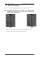
3.2 Rear Panel Connectors 3.2 TRANSMITTER I/O CONNECTIONS Rear Panel Connectors The exciter and receiver can be supplied with optional rear panel connectors that bring out the more important signals available on P1, the rear panel DB25 connector. Figures 1 and 2 show the rear panel connectors, and Table 4 shows the signals that are brought out to the spade connectors. The spade connectors (2.1x0.6x7mm) are captive/soldered at the labelled points.
4 CHANNEL and TONE FREQUENCY PROGRAMMING 4 Receiver DB25/F RX PCB DESCRIPTION TX PCB Transmitter DB25/F 1, 14 +12V +12V DC SUPPLY +12V 1, 14 2 TXD TX Data TXD 2 15 RXD RX Data RXD 15 3 COR+ Carrier Operate Sw+ PressToTalk input PTT 3 16 COR- Carrier Operate Sw- Tx/Rx output T/R 16 4 TONE Subtone output Hi Z audio input+ AUD+ 4 17 AUDIO Audio output Hi Z audio input- AUD- 17 5 AGND Audio Ground Ext tone input+ TONE+ 5 18 DISC Discriminator output Ext ton
5.1 VCO Section 5 5 CIRCUIT DESCRIPTION Circuit Description The following descriptions should be read as an aid to understanding the block and schematic diagrams given in the appendix of this manual. 5.1 VCO Section The Voltage Controlled Oscillator uses a junction FET Q19 which oscillates at the required transmitter output frequency. Varactor diodes D25 and D26 are used by the PLL circuit to keep the oscillator on the desired frequency.
5 CIRCUIT DESCRIPTION 5.3 Power Amplifier tuning voltage which is smoothed by the loop filter components to bias the V.C.O. varactor diode D3. 5.3 Power Amplifier The 10 mW output from the main board connects to the power amplifier board through a short miniature 50 Ohm coaxial cable. Q2 on the power amplifier board increases the signal to approximately 200 mW. The bias current of Q2 is controlled by Q1 and the power levelling circuitry to adjust the drive to the output module U2.
5.7 Local Microphone Input 5 CIRCUIT DESCRIPTION The bridge configuration allows audio signal inversion by interchanging the positive and negative inputs and minimizes ground loop problems. Both inputs should be connected, with one lead going to the source output pin and the other connected to the source audio ground. 5.7 Local Microphone Input The local microphone input is provided for use with a standard low impedance dynamic microphone.
5 CIRCUIT DESCRIPTION 5.10 PTT and DC Remote Control The outputs of U10a and U10c are connected to the frequency response shaping networks C52, R133 (for 750µs pre-emphasis) and C61, R55 (for flat response). JP7 selects the pre-emphasized or flat response. The audio signal is further amplified 100 times by U7d. U7d also provides the symmetrical clipping required to limit the maximum deviation.
5.11 Microprocessor Controller 5 CIRCUIT DESCRIPTION A DMTX board can also cause the exciter to key up. When a TX (or TTL_TX) signal is received by the DMTX board, it pulls pin 6 of JP15 low, which, in turn asserts the PTT_WIRE_OR signal, causing the microprocessor (U13) to key the exciter up. 5.11 Microprocessor Controller The microprocessor controller circuit uses a single-chip eight bit processor and several support chips.
6 FIELD ALIGNMENT PROCEDURE 6 6.1 Standard Test Condition Field Alignment Procedure The procedures given below may be used to align the transmitter in the field. Normally, alignment is only required when changing operating frequencies, or after component replacement. The procedures below do not constitute an exhaustive test or a complete alignment of the module, but if successfully carried out are adequate in most circumstances.
6.3 TCXO Calibration 6 FIELD ALIGNMENT PROCEDURE 4. Measure the voltage between pins 9 and 1 of the test socket (TUNE V), and adjust C99 to obtain 4.5±0.2V, while the TX LED is ON and the ALARM LED is OFF. 6.3 TCXO Calibration 1. Select a channel at the center frequency (half way between the highest and lowest frequencies for the model in question). 2. Disconnect the Audio input (no signal input). 3. Key the PTT line. 4.
6 FIELD ALIGNMENT PROCEDURE 6.5 Tone Deviation 1. Remove the audio input. 2. Key the transmitter on. 3. Adjust RV3 for the desired deviation in the range 0-1kHz.1 (CTCSS) coding is not to be used, adjust RV3 fully CCW. 6.6 6.6 Deviation If sub-tone Deviation 1. Set RV4 (Line Level) fully clockwise (CW). 2. Set the audio to 1kHz, 0dBm, on the line input. 3. Key the transmitter on.. 4. Adjust RV1 (Set Max. Deviation) for a deviation of 5kHz (2.5kHz for narrow band transmitters). 5.
7.1 Overall description 7 SPECIFICATIONS 3. Adjust RV1 on the power amplifier PCB for the desired power level at the output connector. 2 4. Key the transmitter off. 7 7.1 SPECIFICATIONS Overall Description The transmitter is a 5-25 watt output, frequency synthesised, narrow band FM unit which is normally used to drive a high power amplifier. It can also be used alone in lower power applications. The output power is nominally 25 Watts but can be preset between 5 and 25 watts.
7 SPECIFICATIONS 7.1.5 Microprocessor 7.1.5. Microprocessor A microprocessor is used to control the synthesizer, tone squelch, PTT function and facilitate channel frequency programming. With the standard software, RF Technology modules also provide fault monitoring and reporting. 7.2 Physical Configuration The transmitter is designed to fit in a 19 inch rack mounted sub-frame. The installed height is 4 RU (178 mm) and the depth is 350 mm. The transmitter is 63.5 mm or two Eclipse modules wide. 7.
7 SPECIFICATIONS 7.4 Electrical Specifications 7.4 7.4.1 Electrical Specifications Power Requirements Operating Voltage - 10.5 to 16 Vdc with output power reduced below 12 Vdc Current Drain - 5A Maximum, typically 0.2A Standby Polarity - Negative Ground 7.4.2 Frequency Range and Channel Spacing Frequency 66 - 88 MHz 136 - 160 MHz 148 - 174 MHz * 25 kHz T70A T150A T150B 12.5 kHz* T70AN T150AN T150BN The 25 and 12.5 KHz versions are identical.
7 SPECIFICATIONS 7.4.9 7.4.9 Spuriours and Harmonics Spurious and Harmonics Less than 0.25µW 7.4.10 Carrier and Modulation Attack Time Less than 20ms. Certain models have RF envelope attack and decay times controlled in the range 200µs< tr/f <2ms according to regulatory requirements. 7.4.11 Modulation Type - Two point direct FM with optional pre-emphasis Frequency Response - ±1 dB of the selected characteristic from 300 - 3000 Hz Maximum Deviation - Maximum deviation preset to 2.5 or 5 kHz 7.4.
7.4.19 T/R relay Driver 7 SPECIFICATIONS 7.4.19 T/R Relay Driver An open collector transistor output is provided to operate an antenna change over relay or solid state switch. The transistor can sink up to 250mA. 7.4.20 Channel Select Input / Output Coding - 8 lines, BCD coded 00 - 99 Logic Input Levels - Low for <1.5V, High for >3.5V Internal 10K pull down resistors select channel 00 when all inputs are O/C. 7.4.
7 SPECIFICATIONS 7.5 7.5.1 7.5 Connectors Connectors Antenna Connector Type N Female Mounted on the module rear panel 7.5.2 Power & I/O Connector 25-pin “D” Male Mounted on the rear panel 7.5.
7 SPECIFICATIONS Frequency No Tone 67.0 69.4 71.9 74.4 77.0 79.7 82.5 85.4 88.5 91.5 94.8 97.4 100.0 103.5 107.2 110.9 114.8 118.8 123.0 127.3 131.8 136.5 141.3 146.2 151.4 156.7 159.8 162.2 165.5 167.9 171.3 173.8 177.3 179.9 183.5 186.2 189.9 192.8 196.6 199.5 203.5 206.5 210.7 218.1 225.7 229.1 233.6 241.8 250.3 254.