
Operating instructions


RF Technology PA501 Page 14
A ENGINEERING DIAGRAMS
A Engineering Diagrams
Where engineering diagrams are sufficiently complicated, large scale versions are
included as inserts or fold-outs elsewhere in the manual for reading convenience. If
inserts are missing or damaged, the information is identical to that presented in figures
embedded in the text.
A.1 Block Diagram
Figure 1 shows the block signal flow diagram of the PA501 amplifier.
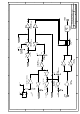
A.2 Circuit Diagrams
Figure 2 shows the detailed circuit diagram of the PA501 amplifier with component
desiquators and values.
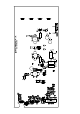
A.3 Component Overlay Diagrams
Figure 3 shows the PCB overlay guide of the PA501 amplifier with component
positions.