
Operating instructions

RF Technology PA501 Page 6
2 CIRCUIT DESCRIPTION
1.4 Amplifier I/O Connections
The PA501 has three connectors on the rear panel.
1.4.1 RF Input
The RF drive is delivered via a BNC connector. The absolute maximum power that
should be applied to this connector is 17 Watts.
1.4.2 RF Output
The RF output signal is available from an N-type connector.
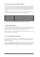
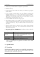
Pins Function
1, 2, 3, 4, 5, 14, 15, 16, 17 Positive supply
9, 10, 11, 12, 13, 22, 23, 24, 25 Ground (negative supply)
8 ALC output
Table 1: Pin connections for the 25 pin “D” connector on the rear panel
Note: The amplifier is capable of delivering as much as 120 Watts continuously.
In certain conditions
1
an RF power of 180 Watts or more can be available via this
connector. This power level can cause burns like any 180w power source.
Appropriate care should be taken when working on the PA501 to avoid making or
breaking connections when the amplifier is operating, and to avoid RF burns
through close proximity to live connections, etc.
1.4.3 25 Pin Connector
The 25-pin “D” connector provides connection to ground and dc power, and from the
automatic level control (ALC) circuit. The pin connections are given in table 1.
2 Circuit Description
The following descriptions should be read as an aid to understanding the block and
schematic diagrams shown in figures 1 and 2.
2.1 Block Overview
The PA501 is comprised of two stages of RF amplification, a directional coupler
sensing forward and reverse power flow, an output low-pass filter and sundry associated
control and monitoring circuitry. The second RF amplifier employs two transistors
operating in parallel, a power splitter following the first RF
____________________
1
Excessive powers may be available, for example, in the event of a failure of the ALC loop,
such as may arise if the ALC feedback connection is broken.