
Operating instructions

RF Technology PA501 Page 8
2.5 Power Control Circuits (Rev 05/9151)
The forward and reverse voltages from the directional coupler are amplified and
inverted by Q103 and Q101. The amplified voltages are compared to preset reference
levels and the comparison signals are combined in a logical fashion by Q109 and Q108
and used to produce the ALC signal. VR137 sets the maximum permitted reverse
power level.
The ALC signal is filtered and supplied to the rear panel system connector for
connection to the ALC control input of an exciter such as the model T500.
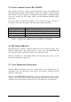
Equipment Type Key Specifications
Power Supply 13.8Vdc, (<25A for 120W)
RF Source 15 Watt source, 450-512MHz, e.g. T500
RF Load / Attenuator
30 dB Attenuator, 50Ω, 150W, SWR<1.2:1
RF Power Meter eg. HP437B or calibrated detector and voltmeter
Table 2: Standard test equipment for the PA501 Power Amplifier
2.6 RF Output Indicator
The forward power voltage is compared with the pre-set dc reference voltage from
VR136 by Q106, Q107. The output of Q113 is used to turn on the RFO LED. The
forward power voltage is buffered to Q116 to turn on the fans via Q6.
VR143 is normally set so that the RFO LED comes ON when output power is 1 - 3db
below the nominal power output level.
2.7 Over Temperature Protection
Thermistor RT144 is mounted to the case of output transistor Q1. If the transistor case
temperature rises above 90 Celsius (about 194
o
F) the resistance of RT144 increases
and Q117 is turned ON.
This causes the TEMP LED and the fans to come on and also reduces the dc output
voltage of the ALC signal via Q109. The input power will then be reduced by the
transmitter ALC circuits and the output transistor is kept within safe operating limits.