RICOH COMPANY,LTD. R5C841 PCI-CardBus/IEEE1394/SD Card /MemoryStick/xD/ExpressCard Data Sheet REV. 1.
RICOH COMPANY,LTD. –REVISION HISTORY– REVISION DATE 0.60 7/24/03 First Draft (described Overview, Block Diagram and Pin description only) 0.70 9/10/03 Addition of the regulator description (Spec 4) and the electrical characteristics (Spec 5). 0.80 11/6/03 Change from NewCard to ExpressCard. Mistakes in writing are corrected. 1.00 1/30/04 First Public Release Mistakes in writing are corrected. 1.10 5/18/04 Changes in the chart of Global Reset Timing (Ch. 5.3.6). Deletion of the 2.
R5C841 PCI-CardBus/IEEE 1394/SD Card/Memory Stick/xD/ExpressCard Data Sheet 1 OVERVIEW The R5C841 is a single chip solution offering five PCI functions (a PCI bus bridge to a PC Card, an IEEE 1394, an SD Card, a Memory Stick and an xD Picture Card) with an ExpressCard (USB Interface Type) switch. PC98/99/2001 compliant PC2001 Design Guide compliant (Subsystem ID, Subsystem Vendor ID) Compliant with ACPI and PCI Bus Power Management 1.
R5C841 PCI-CardBus/IEEE 1394/SD Card/Memory Stick/xD/ExpressCard Data Sheet IEEE1394 Interface Compliant with IEEE1394-1995 Standard Specification and IEEE1394a-2000 Standard Specification Compliant with 1394 OHCI Release 1.1/1.0 Standard Specification Support Cycle Master Provide the Asynchronous receive/transmit FIFO and isochronous receive/transmit FIFO Support Self-ID, physical DMA Data transmission rate of 100, 200 and 400Mbps 2 ports of 1394 Cable interface 24.
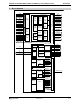
R5C841 PCI-CardBus/IEEE 1394/SD Card/Memory Stick/xD/ExpressCard Data Sheet 2 BLOCK DIAGRAM R5C841 Block Diagram REQ# GNT# IDSEL AD[31:0] C/BE[3:0]# PAR FRAME# DEVSEL# IRDY# TRDY# STOP# PERR# SERR# PCICLK PCIRST# GBRST# CLKRUN# HWSPND# INTA# INTB# INTC# SRIRQ#/UDIO0 UDIO1-UDIO5 RI_OUT#/PME# SPKROUT Socket (Func#0) PCI Interface PCI Address Decode & Mapping CardBus Address Decode & Mapping CardBus Interface Master & Target 16-bit Interface PCI Config.
R5C841 PCI-CardBus/IEEE 1394/SD Card/Memory Stick/xD/ExpressCard 3 3.
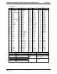
R5C841 PCI-CardBus/IEEE 1394/SD Card/Memory Stick/xD/ExpressCard • Data Sheet CSP Pin List Ball F4 F2 F1 G4 G2 G1 H5 H4 H2 H1 J4 J2 K4 K2 L5 L4 K1 M5 M4 M2 M1 N5 N4 N2 N1 P5 P4 P2 P1 R4 R2 R1 T2 T1 U2 U1 V1 W2 V3 V4 W4 T5 Signal Name TEST HWSPND# SPKROUT RI_OUT#/PME# GBRST# UDIO5 UDIO4 UDIO3 UDIO2 UDIO1 UDIO0/SRIRQ# INTA# INTB# INTC# CLKRUN# PCIRST# PCICLK GNT# REQ# AD31 AD30 AD29 AD28 AD27 AD26 AD25 AD24 C/BE3# IDSEL AD23 AD22 AD21 AD20 AD19 AD18 AD17 AD16 C/BE2# FRAME# IRDY# TRDY# DEVSEL# Pin Name VC
R5C841 PCI-CardBus/IEEE 1394/SD Card/Memory Stick/xD/ExpressCard 3.
R5C841 PCI-CardBus/IEEE 1394/SD Card/Memory Stick/xD/ExpressCard 16-bit Card Interface Pin Name CardBus Card Interface Dir Pin Name Dir Data Sheet Pin Characteristics 5Vtolerant PwrRail Drive IRDY# I/O IRDY# I/O P PCI TRDY# I/O TRDY# I/O P PCI DEVSEL# I/O DEVSEL# I/O P PCI STOP# I/O STOP# I/O P PCI PERR# I/O PERR# I/O P PCI SERR# O (OD) SERR# O (OD) P PCI PAR I/O PAR I/O P PCI C/BE1# I/O C/BE1# I/O P PCI AD15 I/O AD15 I/O P PCI AD14 I/O AD14
R5C841 PCI-CardBus/IEEE 1394/SD Card/Memory Stick/xD/ExpressCard 16-bit Card Interface Pin Name CardBus Card Interface Dir Pin Name Dir Data Sheet Pin Characteristics 5Vtolerant PwrRail Drive Note CE1# O CC/BE0# I/O 3V 4mA CDATA15 I/O CAD8 I/O 3V 4mA CADR10 O CAD9 I/O 3V 4mA CE2# O CAD10 I/O 3V 4mA OE# O CAD11 I/O 3V 4mA VS1# I/O CVS1 I/O 3V 1mA CADR11 O CAD12 I/O 3V 4mA IORD# O CAD13 I/O 3V 4mA CADR9 O CAD14 I/O 3V 4mA IOWR# O CAD15 I/O 3
R5C841 PCI-CardBus/IEEE 1394/SD Card/Memory Stick/xD/ExpressCard 16-bit Card Interface Pin Name CADR0 BVD1/ STSCHG#/ RI# CardBus Card Interface Dir O I (PU) Pin Name CAD26 CSTSCHG Dir Data Sheet Pin Characteristics 5Vtolerant PwrRail Drive I/O 3V 4mA I (PD) 3V – CDATA0 I/O CAD27 I/O 3V 4mA CDATA8 I/O CAD28 I/O 3V 4mA CDATA1 I/O CAD29 I/O 3V 4mA CDATA9 I/O CAD30 I/O 3V 4mA CDATA2 I/O – CDATA10 I/O CAD31 – 3V 4mA I/O 3V 4mA I/O (PU) 3V 4mA WP/ IOIS16# I
R5C841 PCI-CardBus/IEEE 1394/SD Card/Memory Stick/xD/ExpressCard 16-bit Card Interface Pin Name CardBus Card Interface Dir Pin Name Dir Data Sheet Pin Characteristics 5Vtolerant PwrRail XI I XI I AP XO O XO O AP FIL0 I/O FIL0 I/O AP CPS I(PD) CPS Drive I(PD) AP VREF I/O VREF I/O AP REXT I/O REXT I/O AP TPBN0 I/O TPBN0 I/O AP 1394 TPBP0 I/O TPBP0 I/O AP 1394 TPAN0 I/O TPAN0 I/O AP 1394 TPAP0 I/O TPAP0 I/O AP 1394 TPBIAS0 I/O TPBIAS0 I/O AP
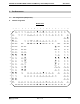
R5C841 PCI-CardBus/IEEE 1394/SD Card/Memory Stick/xD/ExpressCard Data Sheet Small Card Pin Assignments Pin Media I/F SD Card Memory Stick xD Picture Card 1 2 3 4 5 6 7 8 9 10 11 12 13 14 15 16 17 18 19 20 MDIO00 MDIO01 MDIO02 MDIO03 MDIO04 MDIO05 MDIO06 MDIO07 MDIO08 MDIO09 MDIO10 MDIO11 MDIO12 MDIO13 MDIO14 MDIO15 MDIO16 MDIO17 MDIO18 MDIO19 SDCD# — — SDWP# SDPWR0 SDPWR1 SDLED# SDEXTCK SDCCMD SDCCLK SDCDAT0 SDCDAT1 SDCDAT2 SDCDAT3 — — — — — — — MSCD# — — MSPWR — MSLED# MSEXTCK MSBS MSCCLK MSCDAT0
R5C841 PCI-CardBus/IEEE 1394/SD Card/Memory Stick/xD/ExpressCard Pin 16bit Card CardBus ExpressCard 21 22 23 24 25 26 27 28 29 30 31 32 33 34 35 36 37 38 39 40 41 42 43 44 45 46 47 48 49 50 51 52 53 54 55 56 57 58 59 60 61 62 63 64 65 66 67 68 A12 A7 A6 A5 A4 A3 A2 A1 A0 D0 D1 D2 WP/IOIS16# GND GND CD1# D11 D12 D13 D14 D15 CE2# VS1# IORD#/RFU IOWR#/RFU A17 A18 A19 A20 A21 VCC VPP A22 A23 A24 A25 VS2# RESET WAIT# INPACK#/RFU REG# SPKR#/BVD2 STSCHG#/BVD1 D8 D9 D10 CD2# GND CCBE2# CAD18 CAD20 CAD21 CAD2
R5C841 PCI-CardBus/IEEE 1394/SD Card/Memory Stick/xD/ExpressCard Data Sheet Small Card Pin Assignments PC Card Pin (using BAY) PC CARD PIN 1-68 ASSIGNMENTS Pin 16bit Card CardBus SD Card Memory Stick 1 2 3 4 5 6 7 8 9 10 11 12 13 14 15 16 17 18 19 20 21 22 23 24 25 26 27 28 29 30 31 32 33 34 35 36 37 38 39 40 41 42 43 44 45 GND D3 D4 D5 D6 D7 CE1# A10 OE# A11 A9 A8 A13 A14 WE# READY/IREQ# VCC VPP A16 A15 A12 A7 A6 A5 A4 A3 A2 A1 A0 D0 D1 D2 WP/IOIS16# GND GND CD1# D11 D12 D13 D14 D15 CE2# VS1# IORD#
R5C841 PCI-CardBus/IEEE 1394/SD Card/Memory Stick/xD/ExpressCard 3.
R5C841 PCI-CardBus/IEEE 1394/SD Card/Memory Stick/xD/ExpressCard 3.3.1 Data Sheet PCI Local Bus interface signals Pin Name Type Description PCI Bus Interface Pin Descriptions PCICLK IN PCI CLOCK: PCICLK provides timing for all transactions on PCI. All other PCI signals are sampled on the rising edge of PCICLK. CLKRUN# I/O (OD) PCI CLOCK RUN: This signal indicates the status of PCICLK and an open drain output to request the starting or speeding up of PCICLK.
R5C841 PCI-CardBus/IEEE 1394/SD Card/Memory Stick/xD/ExpressCard Pin Name Type Data Sheet Description PCI Bus Interface Pin Descriptions (Continued) 3.3.2 SERR# OUT (OD) SYSTEM ERROR: This signal is pure open drain. The R5C841 actively drives this output for a single PCI clock when it detects an address parity error on either the primary bus or the secondary bus. REQ# OUT (TS) REQUEST: This signal indicates to the arbiter that the R5C841 desires use of the bus. This is a point to point signal.
R5C841 PCI-CardBus/IEEE 1394/SD Card/Memory Stick/xD/ExpressCard 3.3.
R5C841 PCI-CardBus/IEEE 1394/SD Card/Memory Stick/xD/ExpressCard 3.3.4 Data Sheet CardBus PC Card Interface signals Pin Name Type Description CardBus PC Card Interface Pin Descriptions CCLK CCLKRUN# OUT (TS) CardBus Clock: This signal provides timing for all transactions on the PC Card Standard interface and it is an input to every PC Card Standard device.
R5C841 PCI-CardBus/IEEE 1394/SD Card/Memory Stick/xD/ExpressCard Pin Name Type Data Sheet Description CardBus PC Card Interface Pin Descriptions (Continued) 3.3.5 CGNT# OUT CardBus Grant: This signal indicates to the agent that access to the bus has been granted. Every master has its own CGNT#. CPERR# I/O s/h/z CardBus Parity Error: This signal is only for the reporting of data parity errors during all CardBus Card transactions except a Special Cycle.
R5C841 PCI-CardBus/IEEE 1394/SD Card/Memory Stick/xD/ExpressCard 3.3.7 Data Sheet IEEE1394 PHY Interface signals Pin Name Type Description IEEE1394 Cable Interface Pin Descriptions 3.3.8 TPAP1 TPAP0 I/O TPA Positive : Twisted-pair cable A (positive) differential signal terminals. TPBP1 TPBP0 I/O TPB Positive : Twisted-pair cable B (positive) differential signal terminals. TPAN1 TPAN0 I/O TPA Negative : Twisted-pair cable A (negative) differential signal terminals.
R5C841 PCI-CardBus/IEEE 1394/SD Card/Memory Stick/xD/ExpressCard Data Sheet 3.3.10 Small Card Interface signals SD Card Pin Name MDIO Pin Name Type Description SD Card Control Pin Descriptions SDCDAT0 MDIO10 I/O SDCDAT1 MDIO11 I/O SDCDAT2 MDIO12 I/O SDCDAT3 MDIO13 I/O SD Data [3:0] : SD Card 4bit data bus signals. SDCCMD MDIO08 I/O SDCCLK MDIO09 OUT SDWP# MDIO03 IN SD Write Protect : This signal indicates the state of SD card’s write protect switch.
R5C841 PCI-CardBus/IEEE 1394/SD Card/Memory Stick/xD/ExpressCard Data Sheet xD Picture Card Pin Name MDIO Pin Name Type Description xD Picture Card Control Pin Descriptions XDCDAT0 MDIO10 I/O XDCDAT1 MDIO11 I/O XDCDAT2 MDIO12 I/O XDCDAT3 MDIO13 I/O XDCDAT4 MDIO14 I/O XDCDAT5 MDIO15 I/O XDCDAT6 MDIO16 I/O XDCDAT7 MDIO17 I/O XDCLE MDIO18 OUT xD Picture Card CLE : xD Picture Card Command Latch Enable signal.
R5C841 PCI-CardBus/IEEE 1394/SD Card/Memory Stick/xD/ExpressCard Data Sheet 3.3.11 Power and GND signals Pin Name Type Description IN Regulator Enable: This pin controls an internal regulator. Setting this pin to ‘Low’ enables the internal regulator, and setting this pin to ‘High’ disables it. VCC_PCI3V PWR PCI VCC: Power Supply pins for the PCI interface signals. This pin can be powered at 3.3V. VCC_3V PWR 3V VCC : This supply pin is connected to 3.3V.
R5C841 PCI-CardBus/IEEE 1394/SD Card/Memory Stick/xD/ExpressCard Data Sheet 4 FUNCTIONAL DESCRIPTION 4.1 Device Configuration The R5C841 supports PCI-CardBus Bridge Interface functions for the PC Card socket, the PCI-IEEE1394 bridge function, the SD Card interface, the Memory Stick interface and the xD Picture Card interface. Logically the R5C841 looks to the primary PCI as a separate secondary bus residing in a single device.
R5C841 PCI-CardBus/IEEE 1394/SD Card/Memory Stick/xD/ExpressCard Data Sheet 4.1.8 Memory Stick Control Register Space The Memory Stick Control registers are 256byte of register assigned to control the Memory Stick. These registers are used to set for access to the Memory Stick, to give commands and to read/write data. These are placed in the memory mapped I/O space by the Memory Stick Register Base Address register. 4.1.
R5C841 PCI-CardBus/IEEE 1394/SD Card/Memory Stick/xD/ExpressCard Data Sheet 4.3.2 VGA Support The R5C841 supports accesses to the CardBus interface bridge and the VGA compatible devices that is downstream of the bridge. When the VGA Enable bit in the Bridge Control register is set, the R5C841 positively decodes and forwards accesses to VGA frame buffer addresses and I/O accesses to VGA registers from PCI to CardBus interface. The address range is as follows.
R5C841 PCI-CardBus/IEEE 1394/SD Card/Memory Stick/xD/ExpressCard Data Sheet 4.5 Data Buffers, Posting Write, Prefetching Read The R5C841 provides data buffers, address buffers, and command buffers in order to maintain a high-speed data transfer between the PCI bus and the CardBus. The transaction from the PCI bus to the CardBus allows 8-DWORD buffers of Posting Write Data and Prefetching Read Data.
R5C841 PCI-CardBus/IEEE 1394/SD Card/Memory Stick/xD/ExpressCard Data Sheet 4.7 Interrupts The R5C841 supports PCI interrupt signals INTA#, INTB# and INTC# as well as ISA interrupt signals IRQx. They transmit to the system the Card Status Change Interrupt as a card insert/remove event, the Function Interrupt by the PC card, the DMA Interrupt and the Device Interrupt defined on 1394 OHCI, and interrupts defined on SD Card/Memory Stick/xD Picture Card interface.
R5C841 PCI-CardBus/IEEE 1394/SD Card/Memory Stick/xD/ExpressCard Data Sheet Start Frame timing with source sampled a low pulse on IRQ1 SL or H START FRAME H R T IRQ0 FRAME IRQ1 FRAME S S R T R T IRQ2 FRAME S R T PCICLK START1 IRQSER Drive Source 1. IRQ1 Host Controller IRQ1 None None Start Frame pulse can be 4-8 clocks wide.
R5C841 PCI-CardBus/IEEE 1394/SD Card/Memory Stick/xD/ExpressCard Data Sheet 4.8 Card Type Detection If once a valid insertion is detected, the socket state machine in the R5C841 starts to interrogate the PC Card to determine whether it is a CardBus Card, a 16-bit PC Card or an ExpressCard. The R5C841 supports VCC values of 5V, 3.3V and combination of them at the socket interface. Card type can be known by reading the Socket Present State register.
R5C841 PCI-CardBus/IEEE 1394/SD Card/Memory Stick/xD/ExpressCard Data Sheet 4.10 Reset Event Anytime GBRST# is asserted, all R5C841 internal state machines are reset and all registers are set to their default values (provided that each signals has followed the reset sequence below). PCIRST# is asserted, all registers are set to their default value except the following. The default values of each register are described in each register description. 1.
R5C841 PCI-CardBus/IEEE 1394/SD Card/Memory Stick/xD/ExpressCard · 4Ah PME Trigger Enable · ACh Writable Subsystem Vendor ID · AEh Writable Subsystem ID · F8h MS Misc Control · FCh Key xD Picture Card Interface Config Space: · 2Ch Subsystem Vendor ID · 2Eh Subsystem ID · 40h xD Picture Card Clock Control · 4Ah PME Trigger Enable · ACh Writable Subsystem Vendor ID · AEh Writable Subsystem ID · F8h xD Misc Control · FCh Key 1394 OHCI Register: · 24h Global Unique ID High · 28h Global Unique ID Low 1394 PHY R
R5C841 PCI-CardBus/IEEE 1394/SD Card/Memory Stick/xD/ExpressCard Data Sheet ≡Reset Sequence≡ Follow the sequence for initialization when a power is on. 1. Supply a power to VCC_3V, AVCC_PHY3V, VCC_MD3V, VCC_RIN and VCC_ROUT*. (*: in case of an internal regulator disabled ) 2. Supply a power to VCC_PCI3V. 3. Deassert GBRST#. 4. Deassert HWSPND#. 5. Deassert PCIRST#. (PCLK has to be supplied for 100µsec@33MHz before deasserting PCIRST#.) Following Step3 by Step2 has no problem.
R5C841 PCI-CardBus/IEEE 1394/SD Card/Memory Stick/xD/ExpressCard Data Sheet On the software suspend mode, the interface signals on the PC Card keep to the following levels when the card is inserted. CardBus : CCLK=low, CPAR=low, CAD=high or low, CCBE#=high or low, CRST#=low, CGNT#=high, Pull-up=high, Pull-down=low 16-bit : CDATA=hi-z, CADR=low Other pins keep the level before the software suspend mode.
R5C841 PCI-CardBus/IEEE 1394/SD Card/Memory Stick/xD/ExpressCard Data Sheet PHY function On D2 and D3 states, the PHY can be set to any one of the following low power consumption by Software. Select Condition Resume Time Doze Mode Sleep Mode All of Ports status is set to Disconnected, Disabled or Suspended. less than 200ns less than 10ms Doze Mode: Stopping clock of the PHY digital block and getting the Cable Interface’s power down enables the low power consumption.
R5C841 PCI-CardBus/IEEE 1394/SD Card/Memory Stick/xD/ExpressCard Data Sheet 4.13 ZV port Interface The R5C841 has the Bypass type ZV port interface. On the 16-bit interface, when ZV port Enable bit of either the Misc Control 1 register (82Fh) or the PC Card Misc Control 2 register (A0h) is enabled, CADR [25:6], IOIS16#, INPACK#, SPKR# are assigned to ZV port input signal as shown in the below diagram. The R5C841 has no on chip buffer for the ZV port interface.
R5C841 PCI-CardBus/IEEE 1394/SD Card/Memory Stick/xD/ExpressCard 2. Copy of the Subsystem ID and the Subsystem Vendor ID in PCI user defined space method. Card: 1394/SD/MS/xD: 3. Data Sheet C0h, C2h ACh, AEh Load the Subsystem IDs from the Serial ROM method. Connecting SPKROUT to pull-down enables to use the Serial ROM. The R5C841 has the Serial ROM interface, and load the Subsystem ID and the Subsystem Vendor ID after PCI reset disabled. These registers are initialized only by GBRST#. 4.
R5C841 PCI-CardBus/IEEE 1394/SD Card/Memory Stick/xD/ExpressCard Data Sheet 4.16 1394 OHCI The 1394 OHCI block in the R5C841 employs DMA engines for high-performance data transfer, host bus interface and FIFO. The R5C841 supports two types of data transfer: asynchronous and isochronous. Prefer to the 1394 OHCI release 1.1/1.0 specifications for settings and procedures of the controller. 4.16.1 Asynchronous Functions The R5C841 supports all of transmission and reception defined in 1394 packet formats.
R5C841 PCI-CardBus/IEEE 1394/SD Card/Memory Stick/xD/ExpressCard Data Sheet 4.16.4 LINK The Link module sends packets which appear at the transmit FIFO interfaces to the PHY, and places correctly addressed packets into the receive FIFO. The features are as follows. ⋅ ⋅ ⋅ ⋅ ⋅ ⋅ ⋅ ⋅ Transmits and receives correctly formatted 1394 serial bus packets. Generates the appropriate acknowledge for all received asynchronous packets. Performs the cycle master function. Generates and checks 32-bit CRC.
R5C841 PCI-CardBus/IEEE 1394/SD Card/Memory Stick/xD/ExpressCard Data Sheet 4.19.1 Protocol The R5C841 accesses to the xD Picture Card through the 32-bit Data port register. Writing to the Data port register can transfer address, command and data to the xD Picture Card. The data transfer to the xD Picture Card enables in units of 8-bit, 16-bit or 32-bit. On the 16-bit or 32-bit access, the R5C841 can access to the xD Picture Card by increments of 8-bit unit automatically.
R5C841 PCI-CardBus/IEEE 1394/SD Card/Memory Stick/xD/ExpressCard Data Sheet 4.20.3 Format The R5C841 starts accesses to the Serial ROM by detecting a pull-down of the SPKROUT when the first PCI Reset is deasserted after deassertion of the GBRST#. The accessed data is stored to each register as follows. The retry states don’t allow PCI’s slave access during accesses to the Serial ROM.
R5C841 PCI-CardBus/IEEE 1394/SD Card/Memory Stick/xD/ExpressCard Data Sheet 4.20.3.
R5C841 PCI-CardBus/IEEE 1394/SD Card/Memory Stick/xD/ExpressCard Data Sheet 4.20.3.
R5C841 PCI-CardBus/IEEE 1394/SD Card/Memory Stick/xD/ExpressCard Data Sheet 4.20.3.
R5C841 PCI-CardBus/IEEE 1394/SD Card/Memory Stick/xD/ExpressCard Data Sheet 4.21.1 PC Card LED (CardBus R2) The trigger signals of the PC Card LED are as follows. CardBus: R2: CFRAM#, CINT# Card command by IORD#, IOWR#, OE#, WE#, IREQ# Bit 13 and bit 12 of the Config (Func.0) A2h register can set the counter’s duration. bit 13 12 0 1 1 0 0 1 0 1 the LED Output Duration 64 msec (default) 1 msec No Duration Time (through) Test Mode(3.8µsec) 4.21.
R5C841 PCI-CardBus/IEEE 1394/SD Card/Memory Stick/xD/ExpressCard Data Sheet 4.21.5 LED Output Selection All LED can be output to LED0#/LED1#. The LED for the 1394 is output by setting Config (Func.1) 9Eh bit [4:3] to “11b”, the LED for the SD Card is output by setting Config (Func.2) F8h bit [7:6] to “11b”, the LED for the Memory Stick is output by setting Config (Func.3) F8h bit [7:6] to ”11b”, and the LED for the xD Picture Card is output by setting Config (Func.4) F8h bit [7:6] to ”11b”.
R5C841 PCI-CardBus/IEEE 1394/SD Card/Memory Stick/xD/ExpressCard Data Sheet 4.22.2 Transaction of Unused Ports On no use of ports, TPBP* and TPBN* are directly connected to AGND, and TPAP*, TPAN* and TPBIAS* are OPEN. After that, set Port Disable bit of the 1394 PHY Register. The PHY Shadow register in the 1394 Configuration registers space also can set the Port disable bit. See the Read/Write of the 1394PHY register (Ch. 4.22.4). 4.22.
R5C841 PCI-CardBus/IEEE 1394/SD Card/Memory Stick/xD/ExpressCard Data Sheet For example, when 53h is written in wrData of the PHY Control register (bit 6, 4, 1, and 0 are set to “1”), 53h is written in the PHY Register as they are (bit 1, 3, 6, and 7 are set to “1”). Access to Contender bit, Power_class field, and Disable bit for Port0/Port1 in the 1394 PHY register is enabled through the PHY Shadow register (99h) in the 1394 configuration register space.
R5C841 PCI-CardBus/IEEE 1394/SD Card/Memory Stick/xD/ExpressCard Data Sheet 4.22.7 Reference Voltage Circuit and Reference Current Circuit The PHY block of R5C841 supports terminals of the external parts for the Reference voltage circuit and the Reference current circuit. Each terminal should be connected to indicated capacitors and resistors. Reference Voltage Circuit Reference Current Circuit R5C841 VREF R5C841 REXT 0.01uF 10kohm ±1% AGND AGND 4.
R5C841 PCI-CardBus/IEEE 1394/SD Card/Memory Stick/xD/ExpressCard Data Sheet 4.24 Internal Regulator The R5C841 has an internal regulator, which converts the single 3.3V power into the power for the internal core logic. REGEN# signal enables/disables an internal regulator. The following is the recommended circuit diagram. Regulator Disable Mode VCC_RIN R5C841 VCC_ROUT 0.01uF 0.1uF 0.01uF 0.01uF 0.01uF from Regulator (1.8V) 10uF 0.47uF 0.
R5C841 PCI-CardBus/IEEE 1394/SD Card/Memory Stick/xD/ExpressCard Data Sheet 4.25 ExpressCard Interface Using the external USB host interface enables the R5C841 to connect a USB device to a PC Card socket. That is, inserting an ExpressCard passive adapter into the PC Card socket can support an ExpressCard for the USB interface. R5C841 USB HOST ExpressCard Passive Adapter USBDP IORD# USBDM IOWR# USBD+ USBDCPUSB# A22 ExpressCard +3V VCC3EN# Power S/W 4.
R5C841 PCI-CardBus/IEEE 1394/SD Card/Memory Stick/xD/ExpressCard Data Sheet 5 ELECTRICAL CHARACTERISTICS 5.1 Absolute Maximum Rating Symbol Parameter Range Unit Condition Note -0.3 ~ 2.5 V GND=0V 1 Vcc 1 Supply Voltage Range 1 Vcc 2 Supply Voltage Range 2 -0.3 ~ 4.6 V GND=0V 2 Vte1 Voltage on Any Pin -0.3 ~ 5.8 V GND=0V 4 Vte2 Voltage on Any Pin -0.3 ~ 4.
R5C841 PCI-CardBus/IEEE 1394/SD Card/Memory Stick/xD/ExpressCard Data Sheet 5.2.2 PCI Interface For 3.3V signaling (VCC_ROUT= 1.65~1.95V, VCC_PCI3V=3.0~3.6V, Ta=0~70ºC) Symbol Parameter VIH Input High Voltage VIL Input Low Voltage VOH Output High Voltage VOL Output Low Voltage IILk Min Max Unit 0.5xVCC_PCI3V 5.75 V -0.5 0.3xVCC_PCI3V 0.9xVCC_PCI3V Test Condition Note 1 V 1 V Iout=-500µA 1 0.
R5C841 PCI-CardBus/IEEE 1394/SD Card/Memory Stick/xD/ExpressCard Data Sheet 5.2.4 CardBus PC Card Interface (VCC_ROUT= 1.65~1.95V, VCC_3V=3.0~3.6V, Ta=0~70ºC) Symbol Parameter Min Typ Max Unit Test Condition Note VIH Input High Voltage 0.475xVCC_3V VCC_3V +0.5 V 5,6,7 VIL Input Low Voltage -0.5 0.325xVCC_3V V 5,6,7 VOH Output High Voltage VOL Output Low Voltage 0.9xVCC_3V V Iout=-150µA 5,6,8 0.
R5C841 PCI-CardBus/IEEE 1394/SD Card/Memory Stick/xD/ExpressCard Data Sheet 5.2.6 Cable Interface (VCC_ROUT= 1.65~1.95V, AVCC_PHY3V=3.0~3.6V, Ta=0~70ºC) Symbol Parameter VID Differential Input Voltage VICM TpB Common Mode Input Voltage Min Max Unit Test Condition Note 118 260 mV Cable input, during data reception 13,14 168 265 mV Cable input, during arbitration 1.165 2.515 V 100Mbps speed signaling off 0.935 2.515 V 200Mbps speed signaling 14 0.523 2.
R5C841 PCI-CardBus/IEEE 1394/SD Card/Memory Stick/xD/ExpressCard Data Sheet 5.2.8 SD Card Interface (VCC_ROUT= 1.65~1.95V, VCC_MD3V=3.0~3.6V, Ta=0~70ºC) Symbol Parameter Min Typ Max Unit Test Condition Note VIH Input High Voltage 0.625x VCC_MD3V VCC_MD3V +0.3 V 19 VIL Input Low Voltage -0.3 0.25x VCC_MD3V V 19 VOH Output High Voltage VOL Output Low Voltage IIL Input Leakage Current (Pull-up) IOZ HI-Z Output Leakage Current Note 19: Applied for Note 20: Applied for 0.
R5C841 PCI-CardBus/IEEE 1394/SD Card/Memory Stick/xD/ExpressCard Data Sheet 5.2.11 Serial ROM Interface For 3.3V signaling (VCC_ROUT= 1.65~1.95V, VCC_3V=3.0~3.6V, Ta=0~70ºC) Symbol Parameter Min Max Unit Test Condition Note VIL Input Low Voltage -0.5 0.3xVCC_3V V VIH Input High Voltage 0.7xVCC_3V VCC_3V+0.5 V VOL1 Output Low Voltage 0.
R5C841 PCI-CardBus/IEEE 1394/SD Card/Memory Stick/xD/ExpressCard Data Sheet 5.3 AC Characteristics 5.3.1 PCI Interface signals PCI Clock (VCC_ROUT= 1.65~1.95V, VCC_PCI3V=3.0~3.6V, Ta=0~70ºC) Symbol Parameter Min Max Unit Note PCICLK t1a Cycle Time, PCICLK 30 ns t1b Pulse Width Duration, PCICLK High 11 ns t1c Pulse Width Duration, PCICLK Low 11 ns t1d Slew Rate, PCICLK Rising Edge 1 4 V/ns t1e Slew Rate, PCICLK Falling Edge 1 4 V/ns PCICLK Timing t1a t1c t1b *2.0V(0.
R5C841 PCI-CardBus/IEEE 1394/SD Card/Memory Stick/xD/ExpressCard Data Sheet PCI Interface Output Signals (VCC_ROUT= 1.65~1.95V, VCC_PCI3V=3.0~3.6V, Ta=0~70ºC) Symbol Parameter Min Max Unit Note AD [31:0], C/BE#[3:0], PAR, FRAME#, DEVSEL#, IRDY#, TRDY#, STOP#, PERR#, SERR#, CLKRUN# t3a Shared Signal Valid delay time from PCICLK 2 t3b Enable Time, Hi-Z to active delay from PCICLK 2 t3c Disable Time, Active to Hi-Z delay from PCICLK 11 ns Min: CL=0 pF Max: CL=50 pF (10 pF 3.
R5C841 PCI-CardBus/IEEE 1394/SD Card/Memory Stick/xD/ExpressCard Data Sheet 5.3.2 System Interface signals System Interface Signals AC Characteristics (VCC_ROUT= 1.65~1.95V, VCC_PCI3V=3.0~3.6V, VCC_3V=3.0~3.
R5C841 PCI-CardBus/IEEE 1394/SD Card/Memory Stick/xD/ExpressCard Data Sheet 5.3.3 16-bit PC Card Interface signals Memory Read (VCC_ROUT= 1.65~1.95V, VCC_3V=3.0~3.
R5C841 PCI-CardBus/IEEE 1394/SD Card/Memory Stick/xD/ExpressCard Data Sheet Memory Write (VCC_ROUT= 1.65~1.95V, VCC_3V=3.0~3.
R5C841 PCI-CardBus/IEEE 1394/SD Card/Memory Stick/xD/ExpressCard Data Sheet I/O Read (VCC_ROUT= 1.65~1.95V, VCC_3V=3.0~3.
R5C841 PCI-CardBus/IEEE 1394/SD Card/Memory Stick/xD/ExpressCard Data Sheet I/O Write (VCC_ROUT= 1.65~1.95V, VCC_3V=3.0~3.
R5C841 PCI-CardBus/IEEE 1394/SD Card/Memory Stick/xD/ExpressCard Data Sheet 5.3.4 CardBus PC Card Interface signals Clock and Signal Slew Rate (VCC_ROUT= 1.65~1.95V, VCC_3V=3.0~3.
R5C841 PCI-CardBus/IEEE 1394/SD Card/Memory Stick/xD/ExpressCard Data Sheet Card Output (VCC_ROUT= 1.65~1.95V, VCC_3V=3.0~3.
R5C841 PCI-CardBus/IEEE 1394/SD Card/Memory Stick/xD/ExpressCard Data Sheet 5.3.5 Hardware Suspend mode Timing chart for keeping the value of the internal register on the Suspend mode. Hardware Suspend Timing VCC_PCI3V HWSPND# PCI RST# Tpd Tpu Symbol Parameter Min Tpd HWSPND# to PCIRST# delay 100* 1 Typ Max Unit ns Tpu PCIRST# Setup time to HWSPND# 100* 1 ns 1 * : PCICLK=33MHz 5.3.6 Global Reset signals Timing chart for initializing the internal register on the Power’s on.
R5C841 PCI-CardBus/IEEE 1394/SD Card/Memory Stick/xD/ExpressCard Data Sheet 5.3.7 Serial ROM Interface signals SDA (UDIO4), SCL(UDIO3) (VCC_ROUT= 1.65~1.95V, VCC_3V=3.0~3.6V, Ta=0~70ºC) Symbol Parameter Min Max Unit 0 100 kHz Note SDA (UDIO4), SCL (UDIO3) f SCL SCL clock frequency t BUF Bus free time between a STOP and START condition 4.7 - us t HD;STA Hold time (repeated) START condition. After this period, the first clock pulse is generated 4.
R5C841 PCI-CardBus/IEEE 1394/SD Card/Memory Stick/xD/ ExpressCard Data Sheet NOTICE 1. The products and the product specifications described in this Data Sheet are subject to change or discontinuation of production without notice for reasons such as improvement. Therefore, before deciding to use the products, please refer to Ricoh sales representatives for the latest information thereon. 2.
R5C841 PCI-CardBus/IEEE 1394/SD Card/Memory Stick/xD/ ExpressCard RICOH Company, Ltd. Electronic Devices Company ■ Head Office 13-1, Himemurocho, Ikeda-shi, Osaka 563-8501 JAPAN Phone: +81-72-748-6262, Fax: +81-72-753-2120 ■ Yokohama Office 3-2-3, Shinyokohama, Kouhoku-ku, Yokohama-shi, Kanagawa 222-8530 JAPAN Phone: +81-45-477-1703, Fax: +81-45-477-1694 RICOH CORPORATION Electronic Devices Division ■ Cupertino Office 4 Results Way, Cupertino, CA, 95014 USA Phone: 408-346-4463 123452004 REV.1.