VOLTAGE REGULATOR R ×5RL SERIES APPLICATION MANUAL ELECTRONIC DEVICES DIVISION NO.
NOTICE 1. The products and the product specifications described in this application manual are subject to change or discontinuation of production without notice for reasons such as improvement. Therefore, before deciding to use the products, please refer to Ricoh sales representatives for the latest information thereon. 2. This application manual may not be copied or otherwise reproduced in whole or in part without prior written consent of Ricoh. 3.
R × 5RL SERIES APPLICATION MANUAL CONTENTS OUTLINE ......................................................................................................1 FEATURES....................................................................................................1 APPLICATIONS .............................................................................................1 BLOCK DIAGRAM .........................................................................................1 SELCTION GUIDE ..................
VOLTAGE REGULATOR R × 5RL SERIES OUTLINE The R × 5RL Series are voltage regulator ICs with high accuracy output voltage and ultra-low quiescent current by CMOS process. Each of these ICs consists of a voltage reference unit, an error amplifier, a driver transistor, and resistors for setting output voltage. The output voltage is fixed with high accuracy. Three types of packages, TO-92, SOT-89 (Mini-power Mold), SOT-23-5 (Mini-mold), are available. FEATURES • Ultra-low Quiescent Current ....................
SELECTION GUIDE The package type, the output voltage, the packing type, and the taping type of R × 5RL Series can be designated at the user's request by specifying the part number as follows: ↑ a ↑ ↑↑ } } R × 5RL×××× – ×× ← Part Number b cd e ↑ Code Contents a Designation of Package Type: E: TO-92 H: SOT-89 (Mini-power Mold) N: SOT-23-5 (Mini-mold) b Setting Output Voltage (VOUT): Stepwise setting with a step of 0.1V in the range of 2.0V to 6.0V is possible.
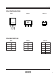
R × 5RL PIN CONFIGURATION • TO-92 • SOT-89 • SOT-23-5 5 (mark side) 4 (mark side) (mark side) 1 1 1 2 2 2 3 3 3 PIN DESCRIPTION • TO-92 • SOT-89 • SOT-23-5 Pin No. Symbol Pin No. Symbol Pin No.
R × 5RL ABSOLUTE MAXIMUM RATINGS Symbol VIN Topt=25˚C Item Rating Input Voltage +12 Unit V VOUT Output Voltage –0.3 to VIN +0.
R × 5RL ELECTRICAL CHARACTERISTICS • R × 5RL20A Symbol Topt=25˚C Item VOUT Output Voltage IOUT Output Current ∆VOUT Load Regulation ∆IOUT VDIF ISS ∆VOUT ∆VIN VIN ∆VOUT ∆Topt Conditions VIN=4.0V 10µA≤IOUT≤10mA VIN=4.0V MIN. TYP. MAX. Unit 1.950 2.000 2.050 V 25 35 VIN=4.0V 1mA≤IOUT≤35mA mA 30 45 mV Dropout Voltage IOUT=1mA 60 90 mV Quiescent Current VIN=4.0V 1.0 3.0 µA 0.05 0.2 %/V 10 V Line Regulation IOUT=1mA VOUT+0.
• R × 5RL40A Symbol Topt=25˚C Item VOUT Output Voltage IOUT Output Current ∆VOUT Load Regulation ∆IOUT VDIF ISS ∆VOUT ∆VIN VIN ∆VOUT ∆Topt Conditions VIN=6.0V 10µA≤IOUT≤10mA VIN=6.0V MIN. TYP. MAX. Unit 3.900 4.000 4.100 V 45 65 VIN=6.0V 1mA≤IOUT≤65mA mA 50 75 mV Dropout Voltage IOUT=1mA 25 38 mV Quiescent Current VIN=6.0V 1.2 3.6 µA 0.05 0.2 %/V 10 V Line Regulation IOUT=1mA VOUT+0.
• R × 5RL60A Symbol Topt=25˚C Item VOUT Output Voltage IOUT Output Current ∆VOUT Load Regulation ∆IOUT VDIF ISS ∆VOUT ∆VIN VIN ∆VOUT ∆Topt Conditions VIN=8.0V 10µA≤IOUT≤10mA VIN=8.0V VIN=8.0V 1mA≤IOUT≤80mA MIN. TYP. MAX. Unit 5.850 6.000 6.150 V 55 80 mA 60 90 mV Dropout Voltage IOUT=1mA 25 38 mV Quiescent Current VIN=8.0V 1.3 3.9 µA 0.05 0.2 %/V 10 V Line Regulation IOUT=1mA VOUT+0.
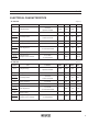
R × 5RL ELECTRICAL CHARACTEISTICS BY OUTPUT VOLTAGE Part Number Conditions R × 5RL20A R × 5RL21A R × 5RL22A R × 5RL23A R × 5RL24A R × 5RL25A R × 5RL26A R × 5RL27A R × 5RL28A R × 5RL29A R × 5RL30A R × 5RL31A R × 5RL32A R × 5RL33A R × 5RL34A R × 5RL35A R × 5RL36A R × 5RL37A R × 5RL38A R × 5RL39A R × 5RL40A R × 5RL41A R × 5RL42A R × 5RL43A R × 5RL44A R × 5RL45A R × 5RL46A R × 5RL47A R × 5RL48A R × 5RL49A R × 5RL50A R × 5RL51A R × 5RL52A R × 5RL53A R × 5RL54A R × 5RL55A R × 5RL56A R × 5RL57A R × 5RL58A R × 5
R × 5RL Topt=25˚C Quiescent Current Line Regulation Iss(µA) ∆VOUT/∆VIN(%/V) Conditions TYP. MAX. Conditions 1.0 3.0 1.1 3.3 TYP. MAX. Input Voltage Output Voltage Tempco. VIN(V) MAX. ∆VOUT/∆T(ppm/˚C) Conditions TYP. IOUT =1mA IOUT VIN =10mA 0.05 VOUT 0.2 10 ±100 =2.0V VOUT+ 1.2 3.6 1.3 3.9 –30˚C≤ 0.
R × 5RL OPERATION VOUT VIN Output Voltage VOUT divided at the node between Registers R1 and R2 is compared with Reference Voltage Error Amplifire by Error Amplifier, so that a constant voltage is output. – R1 + Vref R2 GND GND FIG. 1 Brock Diagram TEST CIRCUITS VIN VIN CI 1µF VOUT R×5RL SERIES + GND ISS IOUT VOUT CI 1µF + Co 1µF P.G R×5RL SERIES VOUT GND FIG. 4 Line Transient Response Test Circuit 10 VOUT + Co 0.1µF + R×5RL SERIES GND FIG.
TYPICAL CHARACTERISTICS 1) Output Voltage vs. Output Current VIN=5.0V 3.1 Topt=–30˚C 2.9 25˚C 80˚C 2.8 2.7 0.0 20 40 60 80 100 Output Current IOUT(mA) 120 Topt=–30˚C 3.9 25˚C 80˚C 3.8 3.7 0.0 0 0 20 40 60 80 100 120 140 160 Output Current IOUT(mA) VIN=7.0V 5.1 Output Voltage VOUT(V) 4.0 Output Voltage VOUT(V) Output Voltage VOUT(V) 3.0 VIN=6.0V 4.1 5.0 Topt=–30˚C 4.9 80˚C 4.8 25˚C 4.7 0.0 0 20 40 60 80 100 120 140 160 Output Current IOUT(mA) 2) Output Voltage vs.
R × 5RL R × 5RL40A 4.2 Topt=25˚C R × 5RL40A 4.05 Topt=25˚C IOUT=1mA 4.0 Output Voltage VOUT(V) Output Voltage VOUT(V) 4.04 IOUT=1mA 3.8 5mA 3.6 10mA 3.4 4.03 4.02 4.01 4.00 3.99 3.98 3.97 3.96 3.2 3.5 4.0 Input Voltage VIN(V) 4 5 6 7 8 Input Voltage VIN(V) R × 5RL50A Topt=25˚C 5.2 5.05 9 10 Topt=25˚C IOUT=1mA 5.04 5.0 Output Voltage VOUT(V) Output Voltage VOUT(V) 3.95 4.5 IOUT=1mA 4.8 5mA 10mA 4.6 4.4 5.03 5.02 5.01 5.00 4.99 4.98 4.97 4.96 4.2 4.5 5.
R × 5RL50A Dropout Voltage VDIF(V) 2.0 1.8 1.6 1.4 1.2 Topt=80˚C 1.0 25˚C 0.8 0.6 –30˚C 0.4 0.2 0.0 0 10 20 30 40 Output Current IOUT(mA) 50 4) Output Voltage vs.Temperature R × 5RL30A VIN=5.0V IOUT=10mA 4.10 3.08 4.08 3.06 4.06 Output Voltage VOUT(V) Output Voltage VOUT(V) 3.10 3.04 3.02 3.00 2.98 2.96 2.94 R × 5RL40A VIN=6.0V IOUT=10mA 4.04 4.02 4.00 3.98 3.96 3.94 2.92 3.92 2.90 0 20 40 60 80 100 –40 –20 Temperature Topt(˚C) 3.
5) Quiescent Current vs. Input Voltage 1.5 1.4 1.4 1.3 1.3 Quiescent Current Iss(µA) Quiescent Current Iss(µA) R × 5RL40A Topt=25˚C 1.5 1.2 1.1 1.0 0.9 0.8 0.7 0.6 0.5 Topt=25˚C 1.2 1.1 1.0 0.9 0.8 0.7 0.6 0.5 3 4 5 6 7 8 Input Voltage VIN(V) R × 5RL50A 2.0 9 10 5 6 7 8 Input Voltage VIN(V) 9 10 Topt=25˚C Quiescent Current Iss(µA) 1.9 1.8 1.7 1.6 1.5 1.4 1.3 1.2 1.1 1.0 4 5 6 7 8 Input Voltage VIN(V) 9 10 6) Quiescent Current vs. Temperature R × 5RL30A VIN=5.0V 1.4 1.9 1.
R × 5RL50A 7) Dropout Voltage vs. Set Output Voltage VIN=7.0V 2.5 0.7 0.6 2.3 Dropout Voltage VDIF(V) Quiescent Current Iss(µA) 2.4 2.2 2.1 2.0 1.9 1.8 1.7 1.6 1.5 –40 –20 0 20 40 60 Temperature Topt(˚C) 0.5 0.4 0.3 IOUT=10mA 0.2 5mA 0.1 1mA 0.0 80 100 0 1 2 3 4 5 Set Output Voltage Vreg(V) 6 8) Line Transient Response (1) IOUT=1mA 8.0 Input Voltage/Output Voltage(V) Input Voltage 7.5 7.0 6.5 6.0 5.5 Output Voltage 5.0 4.5 4.
R × 5RL TYPICAL APPLICATION In R × 5RL Series, a constant voltage can be obtained VIN VIN C1 + R×5RL SERIES without using Capacitors C1 and C2. However, when the VOUT VOUT + wire connected to Vin is long, use Capacitor C1. Output noise can be reduced by using Capacitor C2. C2 GND Insert Capacitors C1 and C2 with the capacitance of 0.1µF to 2.0µF between Input/Output Pins and GND Pin GND GND with minimum wiring.
R × 5RL • CURRENT BOOST CIRCUIT Output current of 60mA or more can be obtained by Tr.1 the current boost circuit constructed as shown in this cirVIN VIN R×5RL SERIES VOUT + C1 cuit diagram. VOUT + GND C2 GND GND • CURRENT BOOST CIRCUIT WITH OVERCURRENT LIMIT CIRCUIT A circuit for protecting Tr.1 from the destruction caused by output short-circuit or overcurrent is shown in Tr.1 R2 this circuit diagram. Vbe2 Tr.
R × 5RL PACKAGE DIMENSIONS (Unit: mm) · SOT-89 · TO-92 4.5±0.1 4.2MAX. 5.2MAX. 1.5±0.1 0.5MAX. 1 4.25MAX. 2.5±0.1 3 2 0.4±0.1 0.8 MIN. 0.7 0.55MAX. ø1.0 12.7MAX. 0.6MAX. 5.2MAX. 2.3MAX. 0.4 1.6±0.2 0.4±0.1 1 3 2 1.27 2.54 · SOT-23-5 2.9±0.2 +0.2 1.1 –0.1 1.9±0.2 (0.95) 0.2 MIN. 4 +0.2 1.6 –0.1 5 0.8±0.1 1 2 0.4±0.1 18 2.8±0.3 (0.95) 0 to 0.1 3 +0.1 0.15 –0.05 0.42 ±0.1 0.47 ±0.1 1.5±0.1 1.5±0.1 0.42 ±0.
R × 5RL TAPING SPECIFICATIONS (Unit: mm) · TO-92 * RR When TZ type tape is pulled out from the direction F 2.3 MAX. 5.2 MAX. 0.7 0.5 MAX. 0.55 MAX. : Mark Side * RF 0.6 MAX. 12.7 MAX. 24.7 MAX. 16.0±0.5 0.7±0.2 ø 4.0±0.2 12.7 ± 0.3 When TZ type tape is pulled out from the direction B 4.2 MAX. 1.45 MAX. 18.0 +1.0 –0.5 9.0±0.5 6.0±0.5 19.0±0.5 5.2 MAX. 0.5 MAX. 12.7 ±1.0 2.5 +0.4 –0.
RICOH COMPANY, LTD. ELECTRONIC DEVICES DIVISION HEADQUARTERS 13-1, Himemuro-cho, Ikeda City, Osaka 563-8501, JAPAN Phone 81-727-53-1111 Fax 81-727-53-6011 YOKOHAMA OFFICE (International Sales) 3-2-3, Shin-Yokohama, Kohoku-ku, Yokohama City, Kanagawa 222-8530, JAPAN Phone 81-45-477-1697 Fax 81-45-477-1694 · 1695 http://www.ricoh.co.jp/LSI/english/ RICOH CORPORATION ELECTRONIC DEVICES DIVISION SAN JOSE OFFICE 3001 Orchard Parkway, San Jose, CA 95134-2088, U.S.A.