
User's Manual

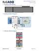


BMD-100 Module Datasheet
Bluetooth 4.1 LE
1/5/2014
BMD-100-DS-V0.5 PRELIMINARY Page 6 of 17
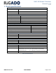
7. Electrical Specifications
7.1. Absolute Maximum Ratings
Symbol
Parameter
Min.
Max.
Unit
V
CC_MAX
Voltage on supply pin
-0.3
3.9
V
V
IO_MAX
Voltage on SXTAL pins
-0.3
1.4
V
T
S
Storage Temperature Range
-40
125
°C
V
ESD-HBM
Electrostatic discharge voltage
-2.0
2.0
kV
Table 4 – Absolute Maximum Ratings
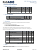
7.2. Operating Conditions
Symbol
Parameter
Min.
Max.
Unit
V
CC
Operating supply voltage
1.7
3.6
V
T
A
Operating Ambient Temperature Range
-40
85
°C
Table 5 – Operating Conditions
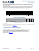
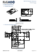
7.3. SPI Interface
The application controller interface (ACI) uses a standard SPI slave interface as the transport
Layer on five physical wires:
2 control wires (clock and slave select)
2 data wires with serial shift-out (MOSI and MISO) in full duplex
1 wire to indicate data availability from the slave
All the SPI pins have an internal pull-down except for the SPI_CS that has a pull-up. All the SPI
pins, except the SPI_CS, are in high impedance state during the low-power states. The SPI_IRQ pin
requires an external pull-down resistor.
Symbol
Parameter
Min.
Typ.
Max.
Unit
F
MAX
SPI Clock Max Frequency
8
MHz
T
RISE
Rise Time
5
-
19
ns
T
FALL
Fall Time
6
-
22
ns
V
IH
Input High Voltage
0.65 x V
CC
-
V
CC
V
V
IL
Input Low Voltage
V
SS
-
0.35 x V
CC
V
V
OH
Output High Voltage (Vcc = 3.3V)
2.4
-
-
V
V
OL
Output Low Voltage (Vcc = 3.3V)
-
-
0.4
V
R
PU
Pull-up Resistance
11
13
16
kΩ
R
PD
Pull-down Resistance
11
13
16
kΩ
Table 6 – SPI Interface
7.4. Clocks
The BMD-100 integrates two low-speed frequency oscillators (LSOSC) and two high-speed
(32 MHz) frequency oscillators (HSOSC).