
User's Manual


BMD-300 Series Module Datasheet
Bluetooth 4.2 LE
October 20, 2016
BMD-300-Series-DS V1.7 Page 7 of 34
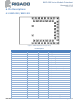
Pin
Name
Direction
Description
34
P0.16
In/Out
GPIO/TRACEDATA[1]
35
P0.17
In/Out
GPIO
36
P0.18
In/Out
GPIO/TRACEDATA[0]/SWO
37
P0.19
In/Out
GPIO
38
P0.20
In/Out
GPIO/TRACECLK
39
P0.21
In/Out
GPIO/RESET
40
P0.22
In/Out
GPIO
2
41
P0.23
In/Out
GPIO
2
42
P0.24
In/Out
GPIO
2
43
SWCLK
In
SWD Clock
44
SWDIO
In/Out
SWD IO
17
VCC
Power
+1.7V to +3.6V
1
1, 2, 3, 4, 5, 16, 18, 29,
30, 45, 46, 47
GND
Power
Electrical Ground
Note 1: An internal 4.7µF bulk capacitor is included on the module. However, it is good design practice to add additional
bulk capacitance as required for your application, i.e. those with heavy GPIO usage and/or current draw.
Note 2: These pins are in close proximity to the nRF52 radio power supply and antenna pins. Radio performance
parameters, such as sensitivity, may be affected by high frequency digital I/O with large sink/source current on these
pins. Nordic recommends using only low frequency, low-drive functions when possible.
Table 3 – BMD-300/301 Pin Descriptions
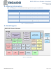
6.2 BMD-350
Figure 3 – BMD-350 Pin out (Top View)
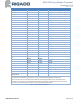
Pin description
Pin
Name
Direction
Description
4
SWCLK
In
SWD Clock
5
SWDIO
In/Out
SWD IO
6
P0.20
In/Out
GPIO/TRACECLK
7
P0.21
In/Out
GPIO/RESET