
Data Sheet
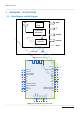
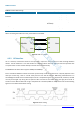
Table Of Contents

R8002 Datasheet
-1
0-
The device on-chip I2C logic provides the serial interface that meets the I2C bus standard mode specification. The I2C
port handles byte transfers autonomously. The I2C H/W interfaces to the I2C bus via two pins: SDA and SCL. Pull up
resistor is needed for I2C operation as these are open drain pins. When the I/O pins are used as I2C port, user must set
the pins function to I2C in advance.
4.3.3 USB Device Controller
USB2.0 fullspeed,4Eps, support host mode.
5. ELECTRICAL CHARACTERISTICS
5.1 Absolute Maximum Ratings
Absolute maximum ratings for supply voltage and voltages on digital and analogue pins of the module are listed below.
Exceeding these values causes permanent damage.
The average PIO pin output current is defined as the average current value flowing through any one of the
corresponding pins for a 100mS period. The total average PIO pin output current is defined as the average current
value flowing through all of the corresponding pins for a 100mS period. The maximum output current is defined as the
value of the peak current flowing through any one of the corresponding pins.
Table 4: Absolute Maximum Rating
Parameter
Min
Max
Unit
VDD_3V3 DC Power Supply -0.3 +3.6 V
T
A
- Operating Temperature -20 +85 °C
T
ST
- Storage Temperature -20 +85 °C
5.2 Recommended Operating Conditions
Table 5: Recommended Operating Conditions
Parameter
Min
Type
Max
Unit
VDD_3V3 DC Power Supply
3.3
-
3.6
V
T
A
- Operating Temperature
-20
25
+85
°C
T
ST
- Storage Temperature -20 25 +85 °C
VIH High Level VDD_3V3-0.3 VDD_3V3+0.3 V
VIL Low Level VSS VSS+0.3 V
VOH High Level VDD_3V3-0.3 VDD_3V3+0.3 V
VOL Low Level VSS VSS+0.3 V
5.3 RF characteristics
Table 6: Transmitter Characteristics
Parameter
Min
Type
Max
Unit
Operating Frequency
2402
2480
MHz
RF output power -20 0 0 dBm
Shenzhen Feasycom Technology Co.,Ltd