
Datasheet

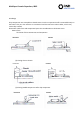

12.3. Land Pattern
When capacitors are mounted on P.C. board, the amount of solder directly affect the
performance of capacitors. Therefore, the following items should be carefully
considered in the design of solder land pattern.
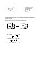
(2) When two or more capacitors are soldered
together onto the same land or pad, the
pad must be designed so that each capacitor’s soldering point is separated by solder-
resist.
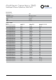
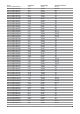
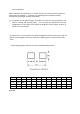
The following diagram and table for recommended pad dimensions.
Type 0201 0402 0603 12060805 1210 1808
1812 1825 2220 2225
D1 0.65 1.50
2.30 2.80 4.00 4.00 5.40 5.30 5.30 7.00 7.00
D2 0.21 0.50
0.80 0.90 0.90 0.90 1.05 0.90 0.90 1.35 1.35
D3 0.23 0.50
0.70 1.00 2.20 2.20 3.30 3.50 3.50 4.30 4.30
D5 0.30 0.50
0.80 1.30
1.60 2.50 2.30 3.80 6.50 5.00 6.50
Unit: mm
(1) The greater the amount of solder,
the higher the stress on the chip capacitors, and
lead to cracking and breaking likely. It is necessary the appropriate size and
configuration of the solder pads should be designed to have proper amount of
solder on the termination.