
Hardware Ref, Installation, and Troubleshooting User guide


2Ć12
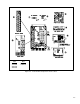
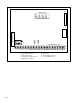
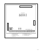
2.7.1 Jumper Locations and Settings
Jumpers
J4 and J17 on the Regulator board are factory
Ćset for voltage in and voltage out signals.
Refer to figures 2.8 and 2.9 for their locations on the Regulator boards. If you need to change the
jumpers' settings, use the following procedures.
CAUTION:
Do not alter the setting of any jumper not described in this
instruction manual. F
ailure to observe
this
precaution could result in damage to or destruction of the equipment.
2.7.1.1 Analog
Input Speed Reference Jumper
Jumper
J4 is the analog speed/torque (U
.000) reference jumper
. This jumper selects either
+/- 10 VDC or 0Ć20 mA input. P
arameters P
.009, P.010, and P
.011 are used in conjunction with the
jumper
. Note that if the position of jumper J4 is changed after the parameters are programmed, the
software will not recognize that the input reference or polarity has been changed. Be sure to verify
that parameters P
.009, P.010, and P
.011 are correct before starting the drive. Refer to instruction
manual D2Ć3339 for more information.
Use the following procedure to set jumper J4:
DANGER
DĆC BUS CAPACITORS RETAIN HAZARDOUS VOLTAGES AFTER INPUT POWER HAS BEEN
DISCONNECTED.
AF
TER DISCONNECTING INPUT POWER
, W
AIT FIVE (5) MINUTES FOR THE D
ĆC
BUS CAPACITORS TO DISCHARGE AND THEN CHECK THE VOLTAGE WITH A VOLTMETER TO
ENSURE THE DĆC BUS CAPACITORS ARE DISCHARGED BEFORE TOUCHING ANY INTERNAL
COMPONENTS. FAILURE TO OBSERVE THIS PRECAUTION COULD RESULT IN SEVERE BODILY
INJURY OR LOS
S OF LIFE
.
Step 1. T
urn off input power to the drive and wait five minutes.
Step 2.
Remove the cover from the drive by unscrewing the four attaching screws.
Step 3. V
erify that the D
ĆC bus voltage is zero by following the procedure in section 9.3.
Step 4.
Locate jumper J4 on the Regulator board. Refer to figures 2.8 and 2.9.
Step 5.
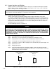
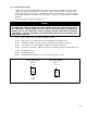
Locate pin 1 on jumper J4. Move the jumper to the desired setting as shown in figure 2.10.
Step 6.
ReĆattach the cover
.
Step 7. ReĆapply input power.
Step 8. V
erify that T
erminal Strip Analog Input Offset (P
.009), T
erminal Strip Analog Input Gain
(P.010), and T
erminal Strip Analog Input Invert (P
.011) are correctly set. Refer to instruction
manual D2Ć3339 for more information.
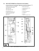
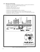
J4 J4
+10 VDC
Pins 2Ć3 Pins 1Ć2
0Ć20 mA
(default)
Voltage
Input Option
Current Input Option
Figure 2.10 Ć Jumper J4 Settings for Analog Input Speed Reference