
Instruction Manual
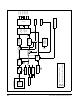

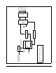
Table Of Contents
- S-3056-1 Distributed Power System SA3100 Drive Configuration and Programming Instruction Manual
- Important User Information
- Contents
- List of Figures
- List of Tables
- Chapter 1 Introduction
- Chapter 2 Configuring the UDC Module, Regulator Type, and Parameters
- 2.1 Adding a Universal Drive Controller (UDC) Module
- 2.2 Entering the Drive Parameters
- 2.3 Configuring the Vector with Constant Power Regulator
- 2.4 Configuring the Volts per Hertz (V/Hz) Regulator
- 2.5 Configuring Flex I/O
- 2.6 Generating Drive Parameter Files and Printing Drive Parameters
- Chapter 3 Configuring the UDC Module’s Registers
- 3.1 Register and Bit Reference Conventions Used in this Manual
- 3.2 Flex I/O Port Registers (Registers 0-23)
- 3.3 UDC/PMI Communication Status Registers (Registers 80-89/1080-1089)
- 3.4 Command Registers (Registers 100-199/1100-1199)
- 3.5 Feedback Registers (Registers 200-299/1200-1299)
- 3.6 Application Registers (Registers 300-599, Every Scan) (Registers 1300-1599, Every Nth Scan)
- 3.7 UDC Module Test I/O Registers (Registers 1000-1017)
- 3.8 Interrupt Status and Control Registers (Registers 2000-2047)
- Chapter 4 Application Programming for DPS Drive Control
- Chapter 5 On-Line Operation
- Appendix A SA3100 Vector Regulator Register Reference
- Appendix B SA3100 Volts / Hertz Regulator Register Reference
- Appendix C SA3100 Local Tunable Variables
- Appendix D Vector with Constant Power Regulator
- Appendix E Volts per Hertz (V/Hz) Regulator
- Appendix F Status of Data in the AutoMax Rack After a STOP_ALL Command or STOP_ALL Fault
- Appendix G Torque Overload Ratio Parameter Precautions
- Appendix H Default Carrier Frequency and Carrier Frequency Limit for Drive Horsepower Ranges
- Appendix I Vector with Constant Power Parameter Entry Example
- Index
SA3100 Local Tunable Variables
C-9
C.6 Resolver Balance and Gain Variables
The resolver gain and balance variable values are used to compensate for varying
lengths of resolver wiring. The balance value can be generated automatically by
commanding the resolver calibration test in register 101/1101. The gain value will be
generated automatically when the RES_GAN% variable is equal to zero., i.e., on
power-up. Refer to the SA3100 PMI Regulator instruction manual (S-3057) for more
information on the calibration procedures.
Note that Distributed Power Systems are designed to be used with the resolvers
described in S-3057. The validity of the results of these calibration procedures are not
guaranteed if resolvers other than those described are used.
Figure C.1 – Capacitance Used for Resolver Balancing
VRT_E0% Voltage Ripple Warning Threshold
A drive warning is generated (203/1203, bit 3) if
ripple (voltage variation) on the DC bus
exceeds the value stored in this variable. The
value is entered in volts.
Units: Volts
Default Value: 20
Low Limit: 10
High Limit: 24
Step: 1
This diagnostic is operational after the bus has reached steady state. It is intended
to be used to detect an input phase loss in the rectifier section of a three-phase AC
input. However, it can also be used with a common bus supply.
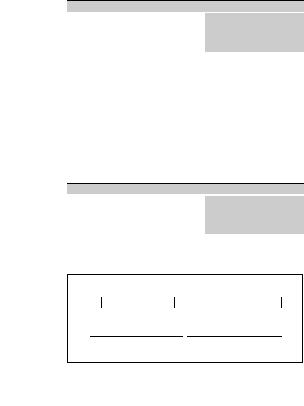
RES_BAL% Resolver Balance
The RES_BAL% local tunable contains the
amount of capacitance that is to be added to
the sine or cosine channel of the resolver to
compensate for stray inductance in the wiring.
Units: pF
∗
100
Default Value: 0
Low Limit: 0
High Limit: 79
Step: 1
This value may range from 0 to 79, with 0 indicating that balance tuning has not
been performed. Values from 1 to 39 add capacitance to the cosine channel, while
values from 41 to 79 add capacitance to the sine channel. Each integer value
represents 100 pF as shown in figure C.1.
Added to Cosine Channel
Added to Sine Channel
3900 pF
100 pF 0 pF 100 pF
3900 pF
01
39 40 41
79
Tuning
Not Done