
Instruction Manual
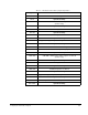
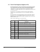
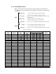
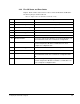
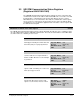
Table Of Contents
- S-3056-1 Distributed Power System SA3100 Drive Configuration and Programming Instruction Manual
- Important User Information
- Contents
- List of Figures
- List of Tables
- Chapter 1 Introduction
- Chapter 2 Configuring the UDC Module, Regulator Type, and Parameters
- 2.1 Adding a Universal Drive Controller (UDC) Module
- 2.2 Entering the Drive Parameters
- 2.3 Configuring the Vector with Constant Power Regulator
- 2.4 Configuring the Volts per Hertz (V/Hz) Regulator
- 2.5 Configuring Flex I/O
- 2.6 Generating Drive Parameter Files and Printing Drive Parameters
- Chapter 3 Configuring the UDC Module’s Registers
- 3.1 Register and Bit Reference Conventions Used in this Manual
- 3.2 Flex I/O Port Registers (Registers 0-23)
- 3.3 UDC/PMI Communication Status Registers (Registers 80-89/1080-1089)
- 3.4 Command Registers (Registers 100-199/1100-1199)
- 3.5 Feedback Registers (Registers 200-299/1200-1299)
- 3.6 Application Registers (Registers 300-599, Every Scan) (Registers 1300-1599, Every Nth Scan)
- 3.7 UDC Module Test I/O Registers (Registers 1000-1017)
- 3.8 Interrupt Status and Control Registers (Registers 2000-2047)
- Chapter 4 Application Programming for DPS Drive Control
- Chapter 5 On-Line Operation
- Appendix A SA3100 Vector Regulator Register Reference
- Appendix B SA3100 Volts / Hertz Regulator Register Reference
- Appendix C SA3100 Local Tunable Variables
- Appendix D Vector with Constant Power Regulator
- Appendix E Volts per Hertz (V/Hz) Regulator
- Appendix F Status of Data in the AutoMax Rack After a STOP_ALL Command or STOP_ALL Fault
- Appendix G Torque Overload Ratio Parameter Precautions
- Appendix H Default Carrier Frequency and Carrier Frequency Limit for Drive Horsepower Ranges
- Appendix I Vector with Constant Power Parameter Entry Example
- Index
3-8
SA3100 Drive Configuration and Programming
3.2.2 Analog Data Formats
Data is returned from the Flex I/O module’s analog-to-digital converter with 12-bit
resolution. The value is left-justified into a 16-bit field, reserving the most significant bit
for a sign bit.
A/D Unipolar Data
11 10 09 08 07 06 05 04 03 02 01 00
⇓⇓⇓⇓⇓⇓⇓⇓⇓⇓⇓⇓
Analog Value 0*141312111009080706050403020100
Input
* = Always positive
A/D Bipolar Data S 10 09 08 07 06 05 04 03 02 01 00
⇓⇓⇓⇓⇓⇓⇓⇓⇓⇓⇓
Analog Value S 14 13 12 11 10 09 08 07 06 05 04 03 02 01 00
D/A Data
S 111009080706050403020100
Output
⇓⇓⇓⇓⇓⇓⇓⇓⇓⇓⇓⇓
Analog Value S 14 13 12 11 10 09 08 07 06 05 04 03 02 01 00
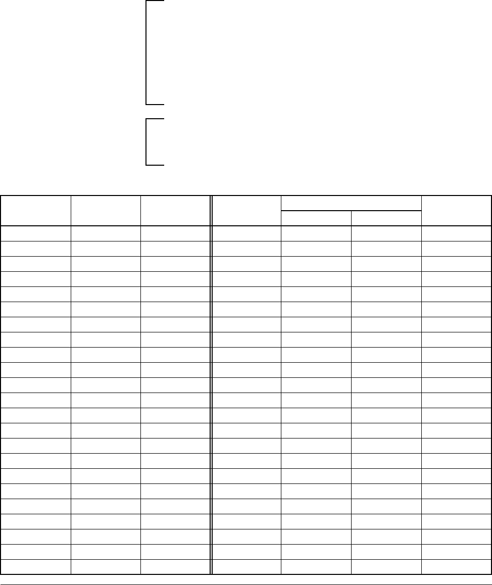
Table 3.5 – Analog Data
Current
(mA)
4-20mA
Mode
0-20mA
Mode Voltage (V)
+/- 10 Volt Mode
0-10 Volt
ModeInput Output
-10.5 -32768 -32768
0 0 -10.0 -31200 -31208
1 1560 -9.0 -28080 -28088
2 3120 -8.0 -24960 -24968
3 4680 -7.0 -21840 -21848
4 0 6240 -6.0 -18720 -18728
5 1927 7800 -5.0 -15600 -15608
6 3854 9360 -4.0 -12480 -12488
7 5782 10920 -3.0 -9360 -9368
8 7710 12480 -2.0 -6240 -6248
9 9637 14040 -1.0 -3120 -3128
10 11565 15600 0 0 0 0
11 13492 17160 1.0 3120 3120 3120
12 15420 18720 2.0 6240 6240 6240
13 17347 20280 3.0 9360 9360 9360
14 19275 21840 4.0 12480 12480 12480
15 21202 23400 5.0 15600 15600 15600
16 23130 24960 6.0 18720 18728 18728
17 25057 26520 7.0 21840 21848 21848
18 26985 28080 8.0 24960 24968 24968
19 28912 29640 9.0 28080 28088 28088
20 30840 31200 10.0 31200 31208 31208
21 32767 32760 10.5 32752 32760 32760