
Instruction Manual
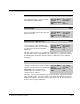
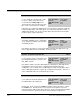
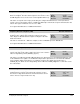
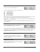
Table Of Contents
- S-3056-1 Distributed Power System SA3100 Drive Configuration and Programming Instruction Manual
- Important User Information
- Contents
- List of Figures
- List of Tables
- Chapter 1 Introduction
- Chapter 2 Configuring the UDC Module, Regulator Type, and Parameters
- 2.1 Adding a Universal Drive Controller (UDC) Module
- 2.2 Entering the Drive Parameters
- 2.3 Configuring the Vector with Constant Power Regulator
- 2.4 Configuring the Volts per Hertz (V/Hz) Regulator
- 2.5 Configuring Flex I/O
- 2.6 Generating Drive Parameter Files and Printing Drive Parameters
- Chapter 3 Configuring the UDC Module’s Registers
- 3.1 Register and Bit Reference Conventions Used in this Manual
- 3.2 Flex I/O Port Registers (Registers 0-23)
- 3.3 UDC/PMI Communication Status Registers (Registers 80-89/1080-1089)
- 3.4 Command Registers (Registers 100-199/1100-1199)
- 3.5 Feedback Registers (Registers 200-299/1200-1299)
- 3.6 Application Registers (Registers 300-599, Every Scan) (Registers 1300-1599, Every Nth Scan)
- 3.7 UDC Module Test I/O Registers (Registers 1000-1017)
- 3.8 Interrupt Status and Control Registers (Registers 2000-2047)
- Chapter 4 Application Programming for DPS Drive Control
- Chapter 5 On-Line Operation
- Appendix A SA3100 Vector Regulator Register Reference
- Appendix B SA3100 Volts / Hertz Regulator Register Reference
- Appendix C SA3100 Local Tunable Variables
- Appendix D Vector with Constant Power Regulator
- Appendix E Volts per Hertz (V/Hz) Regulator
- Appendix F Status of Data in the AutoMax Rack After a STOP_ALL Command or STOP_ALL Fault
- Appendix G Torque Overload Ratio Parameter Precautions
- Appendix H Default Carrier Frequency and Carrier Frequency Limit for Drive Horsepower Ranges
- Appendix I Vector with Constant Power Parameter Entry Example
- Index

Configuring the UDC Module’s Registers
3-31
I/O Status Register (Continued) 201/1201
Auxiliary Input 5 Bit 5
The Auxiliary Input 5 bit reflects the status of
the 115 VAC auxiliary input 5 on the
Resolver & Drive I/O board. When the input
signal is present, this bit is set.
Hex Value: 0020H
Sug. Var. Name: AUX_IN5@
Access: Read only
UDC Error Code: N/A
LED: AUX IN5
Resolver Gain Calibrated Bit 6
The Resolver Gain Calibrated status bit is
set when the resolver gain calibration
procedure is complete. This procedure is
performed when the value stored in local
tunable RES_GAN% is set to zero.
Hex Value: 0040H
Sug. Var. Name: RES_GAN@
Access: Read only
UDC Error Code: N/A
LED: N/A
Resolver Balance Calibrated Bit 7
The Resolver Balance Calibrated status bit
is set when the resolver balance calibration
procedure is complete. This procedure is
performed when the Enable Resolver
Calibration Procedure bit (register
101/1101, bit 6) is set and the motor is
tuning.
Hex Value: 0080H
Sug. Var. Name: RES_BAL@
Access: Read only
UDC Error Code: N/A
LED: N/A
External Strobe Detected Bit 8
The External Strobe Detected status bit is
set when the external strobe on the motor’s
resolver is detected. Register 216/1216
displays the position of the resolver at the
time of the strobe.
Hex Value: 0100H
Sug. Var. Name: STR_DET@
Access: Read only
UDC Error Code: N/A
LED: N/A
Note that this bit is set for only one scan, allowing a strobe to be detected every
scan. The UDC task must check the External Strobe Detected bit each scan to
ensure the validity of the strobe data in register 216/1216.
External Strobe Level Bit 9
The External Strobe Level status bit is set or
reset by the system when the external
strobe is detected. It indicates whether the
external strobe level was rising (1) or
falling (0).
Hex Value: 0200H
Sug. Var. Name: STR_LVL@
Access: Read only
UDC Error Code: N/A
LED: N/A