
Instruction Manual
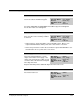
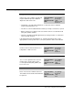
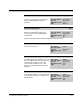
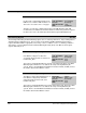
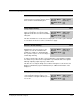
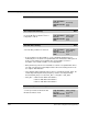
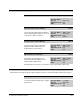
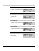
Table Of Contents
- S-3056-1 Distributed Power System SA3100 Drive Configuration and Programming Instruction Manual
- Important User Information
- Contents
- List of Figures
- List of Tables
- Chapter 1 Introduction
- Chapter 2 Configuring the UDC Module, Regulator Type, and Parameters
- 2.1 Adding a Universal Drive Controller (UDC) Module
- 2.2 Entering the Drive Parameters
- 2.3 Configuring the Vector with Constant Power Regulator
- 2.4 Configuring the Volts per Hertz (V/Hz) Regulator
- 2.5 Configuring Flex I/O
- 2.6 Generating Drive Parameter Files and Printing Drive Parameters
- Chapter 3 Configuring the UDC Module’s Registers
- 3.1 Register and Bit Reference Conventions Used in this Manual
- 3.2 Flex I/O Port Registers (Registers 0-23)
- 3.3 UDC/PMI Communication Status Registers (Registers 80-89/1080-1089)
- 3.4 Command Registers (Registers 100-199/1100-1199)
- 3.5 Feedback Registers (Registers 200-299/1200-1299)
- 3.6 Application Registers (Registers 300-599, Every Scan) (Registers 1300-1599, Every Nth Scan)
- 3.7 UDC Module Test I/O Registers (Registers 1000-1017)
- 3.8 Interrupt Status and Control Registers (Registers 2000-2047)
- Chapter 4 Application Programming for DPS Drive Control
- Chapter 5 On-Line Operation
- Appendix A SA3100 Vector Regulator Register Reference
- Appendix B SA3100 Volts / Hertz Regulator Register Reference
- Appendix C SA3100 Local Tunable Variables
- Appendix D Vector with Constant Power Regulator
- Appendix E Volts per Hertz (V/Hz) Regulator
- Appendix F Status of Data in the AutoMax Rack After a STOP_ALL Command or STOP_ALL Fault
- Appendix G Torque Overload Ratio Parameter Precautions
- Appendix H Default Carrier Frequency and Carrier Frequency Limit for Drive Horsepower Ranges
- Appendix I Vector with Constant Power Parameter Entry Example
- Index

3-34
SA3100 Drive Configuration and Programming
Drive Fault Register (Continued) 202/1202
Charge Bus Time-Out Fault Bit 6
The Charge Bus Time-out Fault bit is set to
indicate any of the conditions listed below.
Register 222/1222 provides additional
diagnostics if this fault occurs.
Hex Value: 0040H
Sug. Var. Name: FLT_CHG@
Access: Read only
UDC Error Code: 1024
LED: EXT FLT and
P.M. FLT
• The DC bus is not fully charged within 10 seconds after the bus enable bit
(register 100/1100, bit 4) is set.
• The drive is on and feedback indicates that the pre-charge contactor has opened.
• DC bus voltage is less than the value stored in the Power Loss Fault Threshold
(PLT_E0%) tunable variable.
• The lack of 115VAC or 24V DC applied to the precharge module on common bus
units (C through H-frame).
If the Charge Bus Time-Out Fault bit is set, verify that incoming power is at the
appropriate level. If the power level is correct, the problem is in the Power Module.
Over Temperature Fault Bit 7
The Over Temperature Fault bit is set if the
thermistor in the Power Module detects a
temperature of 100° C or more.
Hex Value: 0080H
Sug. Var. Name: FLT_OT@
Access: Read only
UDC Error Code: 1016
LED: P.M. FLT
Resolver Broken Wire Fault Bit 8
The Resolver Broken Wire Fault bit is set if a
sine or cosine signal from the resolver is
missing due to a broken wire or if the
resolver gain tunable (RES_GAN%) has
been set too low.
Hex Value: 0100H
Sug. Var. Name: FLT_TBW@
Access: Read only
UDC Error Code: 1008
LED: FDBK OK
Resolver Fault Bit 9
The Resolver Fault bit is set if the fuse
blows on the Resolver & Drive I/O board.
This indicates the board has failed and must
be replaced.
Hex Value: 0200H
Sug. Var. Name: FLT_RES@
Access: Read only
UDC Error Code: 1009
LED: N/A