
Datasheet


Technical Note
BA10358F/FV, BA10324AF/FV, BA2904SF/FV/FVM, BA2904F/FV/FVM
BA2902SF/FV/KN, BA2902F/FV/KN, BA3404F/FVM
17/25
www.rohm.com
2010.11 - Rev.
A
© 2010 ROHM Co., Ltd. All rights reserved.
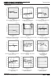
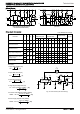
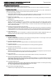
●Circuit Diagram
●Test circuit1 NULL method
VCC,VEE,EK,Vicm
Unit:[V]
Parameter
VF S1 S2 S3
BA10358 family
BA10324A family
BA2904 family
BA2902 family
BA3404 family
calculation
VCC VEE EK Vicm VCC VEE EK Vicm VCC VEE EK Vicm
Input Offset Voltage
VF1 ON ON OFF 5 0 -1.4 0 5~30 0 -1.4 0 15 -15 0 0
1
Input Offset Current
VF2 OFF OFF OFF 5 0 -1.4 0 5 0 -1.4 0 15 -15 0 0
2
Input Bias Current
VF3 OFF ON
OFF 5 0 -1.4 0 5 0 -1.4 0 15 -15 0 0
3
VF4 ON OFF
Large Signal Voltage Gain
VF5
ON ON ON
15 0 -1.4 0 15 0 -1.4 0 15 -15 10 0
4
VF6 15 0 -11.4 0 15 0 -11.4 0 15 -15 -10 0
Common-mode Rejection
Ratio (Input common-mode
Voltage Range)
VF7
ON ON OFF
5 0 -1.4 0 5 0 -1.4 0 15 -15 0 -15
5
VF8 5 0 -1.4 3.5 5 0 -1.4 3.5 15 -15 0 13
Power Supply
Rejection Ratio
VF9
ON ON OFF
5 0 -1.4 0 5 0 -1.4 0 2 -2 0 0
6
VF10 30 0 -1.4 0 30 0 -1.4 0 15 -15 0 0
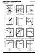
-Calculation-
1. Input Offset Voltage (Vio)
]V[
Rs / Rf + 1
VF1
Vio
2. Input Offset Current (Iio)
]A[
Rs) / Rf + (1× Ri
VF1-VF2
Iio
3. Input Bias Current (Ib)
]A[
Rs) / Rf + (1 ×Ri×2
VF3-VF4
Ib
4. Large Signal Voltage Gain (Av)
]dB[
VF6-VF5
Rf/Rs)+(1×EK
Log×20 Av
Δ
5. Common-mode Rejection Ration (CMRR)
]dB[
VF7-VF8
Rf/Rs)+(1×Vicm
Log×20 CMRR
Δ
6. Power supply rejection ratio (PSRR)
]dB[
VF9-VF10
Rf/Rs)+(1×Vcc
Log×20 PSRR
Δ
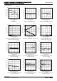
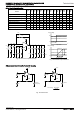
Fig. 120 Schematic Diagram
(BA3404)
Fig. 121 Test circuit1 (one channel only)
+
IN
-
IN
VOU
T
VCC
VEE
VOU
T
-
IN
+
IN
VCC
VEE
Fig. 119 Schematic Diagram
(BA10358/BA10324A/BA2904S/
BA2904/BA2902S/BA2902)
VC
C
C2
0.1[μF]
Rf
50[kΩ]
S1
RiRs
10[kΩ]50[Ω]
10[kΩ]
50[Ω]
Ri
Rs
S2
RL
S3
1000[pF]
C3
500[kΩ]
500[kΩ]
0.1[μF]
R
K
E
K
R
K
C1
+15[V]
-15[V]
NULL
V
V
F
DUT
VE
E
Vic
m