
Datasheet

BD7561G,BD7561SG,BD7541G,BD7541SG,
BD7562F/FVM,BD7562SF/FVM, BD7542F/FVM,BD7542SF/FVM
Technical Note
13/20
www.rohm.com
2009.05 - Rev.A
© 2009 ROHM Co., Ltd. All rights reserved.
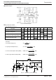
Vio
|VF1|
=
1+Rf/Rs
[V]
A
v
|VF2-VF3|
=
2×
(1+Rf/Rs)
[dB]
20Log
CMRR
|VF4-VF5|
=
1.8×
(1+Rf/Rs)
[dB]
20Log
PSRR
|VF6-VF7|
=
3.8×
(1+Rf/Rs)
[dB]
20Log
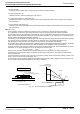
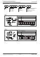
●Schematic diagram
●Test circuit1 NULL method
VDD,VSS,EK,Vicm Unit : [V]
Parameter VF S1 S2 S3 VDD VSS EK Vicm Calculation
Input Offset Voltage VF1 ON ON OFF 12 0 -6 12 1
Large Signal Voltage Gain
VF2
ON ON ON 12 0
-0.5
6 2
VF3 -11.5
Common-mode Rejection Ratio
(Input Common-mode Voltage Range)
VF4
ON ON OFF 12 0 -6
0
3
VF5 12
Power Supply Rejection Ratio
VF6
ON ON OFF
5
0 -2.5 0 4
VF7 14.5
-Calculation-
1. Input Offset Voltage (Vio)
2. Large Signal Voltage Gain (Av)
3. Common-mode Rejection Ratio (CMRR)
4. Power Supply Rejection Ratio (PSRR)
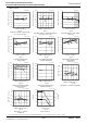
Fig. 94. Test circuit 1 (one channel only)
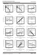
Fig. 93. Schematic diagram
VDD
Rf =50[kΩ]
Ri=1[MΩ]
0.015[μF]
RS
=
50[Ω]
SW2
RL
SW3
500[kΩ]
500[kΩ]
0.01[μF]
E
K
15[V]
DU
T
VSS
VRL50[kΩ]
Vicm
SW1
0.015[μF]
Ri=1[MΩ]
Vo
V
F
RS
=
50[Ω] 1000[pF]
0.1[μF]
-15[V]
NULL
+