
Datasheet


Technical Note
14/21
BR24T□□□-W Series
www.rohm.com
2011.1 - Rev.H
© 2011 ROHM Co., Ltd. All rights reserved.
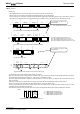
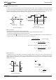
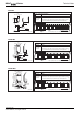
●I/O peripheral circuit
○Pull up resistance of SDA terminal
SDA is NMOS open drain, so requires pull up resistance. As for this resistance value (R
PU
), select an appropriate value to this resistance
value from microcontroller V
IL
, I
L
,
and V
OL
-I
OL
characteristics of this IC. If R
PU
is large, action frequency is limited. The smaller the R
PU
, the
larger the consumption current at action.
○Maximum value of R
PU
The maximum value of R
PU
is determined by the following factors.
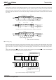
①SDA rise time to be determined by the capacitance (CBUS) of bus line of R
PU
and SDA should be tR or below.
And AC timing should be satisfied even when SDA rise time is late.
②The bus electric potential A to be determined by input leak total (I
L
) of device connected to bus at output of 'H' to SDA bus and R
PU
should sufficiently secure the input 'H' level (V
IH
) of microcontroller and EEPROM including recommended noise margin 0.2Vcc.
VCC-ILRPU-0.2 VCC ≧ VIH
∴
R
PU
≦
0.8V
CC
-
V
IH
I
L
Ex.) V
CC =3V IL=10μA VIH=0.7 VCC
from②
≦
300
[kΩ]
R
PU
≦
0.8×3-0.7×3
10×10
-6
○ Minimum value of R
PU
The minimum value of R
PU
is determined by the following factors.
When IC outputs LOW, it should be satisfied that V
OLMAX
=0.4V and I
OLMAX
=3mA.
②V
OLMAX= should secure the input 'L' level (V
IL
) of microcontroller and EEPROM including recommended noise margin 0.1Vcc.
V
OLMAX ≦ VIL-0.1 VCC
Ex.) V
CC =3V、VOL=0.4V、IOL=3mA、microcontroller, EEPROM V
IL
=0.3Vcc
And V
OL=0.4[V]
V
IL=0.3×3
=0.9[V]
Therefore, the condition ② is satisfied.
○Pull up resistance of SCL terminal
When SCL control is made at CMOS output port, there is no need, but in the case there is timing where SCL becomes 'Hi-Z', add a pull
up resistance. As for the pull up resistance, one of several kΩ ~ several ten kΩ is recommended in consideration of drive performance
of output port of microcontroller.
I
OL
R
PU
≧
V
CC
-
V
OL
I
OL
∴
V
CC
-
V
O
L
R
PU
≦
≧
867
[Ω]
R
PU
≧
3
-
0.4
3×10
-3
from①
Microcontroller
RPU
A
SDA
terminal
I
L
IL
Bus line
capacity
CBUS
Fig.49 I/O circuit diagram
BR24TXX