
Datasheet


Technical Note
14/18
BR25S□□□ Series
www.rohm.com
2010.12 - Rev.B
© 2010 ROHM Co., Ltd. All rights reserved.
●Notes on power ON/OFF
○At standby
Set CSB “H”, and be sure to set SCK, SI input “L” or “H”. Do not input intermediate electric potantial.
○At power ON/OFF
When Vcc rise or fall, set CSB=”H” (=Vcc).
When CSB is “L”, this IC gets in input accept status (active). If power is turned on in this status, noises and the likes may
cause malfunction, erroneous write or so. To prevent these, at power ON, set CSB “H”. (When CSB is in “H” status, all
inputs are canceled.)
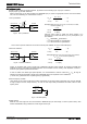
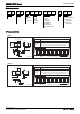
(Good example) CSB terminal is pulled up to Vcc.
At power OFF, take 10ms or more before supply. If power is turned on without observing this condition, the IC
internal circuit may not be reset.
(Bad example) CSB terminal is “L” at power ON/OFF.
In this case, CSB always becomes “L” (active status), and EEPROM may have malfunction or erroneous write owing
to noises and the likes.
Even when CSB input is High-Z, the status becomes like this case.
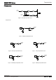
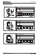
○Operating timing after power ON
As shown in Fig.55, at standby, when SCK is “H”, even if CSB is fallen, SI status is not read at fall edge. SI status is read
at SCK rise edge after fall of CSB. At standby and at power ON/OFF, set CSB “H” status.
○At power on malfunction preventing function
This IC has a POR (Power On Reset) circuit as mistake write countermeasure. After POR action, it gets in write disable
status. The POR circuit is valid only when power is ON, and does not work when power is OFF. When power is ON, if the
recommended conditions of the following tR, tOFF, and Vbot are not satisfied, it may become write enable status owing to
noises and the likes.
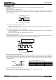
Recommended conditions of t
R
, t
OFF
, Vbot
tR tOFF Vbot
10ms or below 10ms or higher 0.3V or below
100ms or below
10ms or higher 0.2V or below
○Low voltage malfunction preventing function
LVCC (Vcc-Lockout) circuit prevents data rewrite action at low power, and prevents wrong write.
At LVCC voltage (Typ. =1.2V) or below, it prevent data rewrite.
tR
tOFF
Vbo
t
0
Vcc
Fig.54 CSB timing at power ON/OFF
CSB
Vcc
Bad example Good example
Fig.56 Rise waveform
Fig.55 Operating timing
0 1 2
Command start here. SI is read.
Even if CSB is fallen at SCK=”H”,
SI status is not read at that edge.
CSB
SCK
SI