
Datasheet


Technical Note
9/18
BR25S□□□ Series
www.rohm.com
2010.12 - Rev.B
© 2010 ROHM Co., Ltd. All rights reserved.
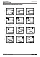
3. Write command (WRITE)
By write command, data of EEPROM can be written. As for this command, set CSB LOW, then input address and data
after write ope code. Then, by making CSB HIGH, the EEPROM starts writing. The write time of EEPROM requires time
of tE/W (Max 5ms). During tE/W, other than read status register command is not accepted. Set CSB HIGH between
taking the last data (D0) and rising the next SCK clock. At the other timing, write command is not executed, and this write
command is cancelled. This IC has page write function, and after input of data for 1 byte (8 bits), by continuing data input
without setting CSB HIGH, 2byte or more data can be written for one tE/W. The maximum number of write bytes is
specified per device of each capacity. Up to 64 arbitrary bytes can be written (in the case of BR25S128/256-W). In page
write, the insignificant 5
bit of the designated address is incremented internally at every time when data of 1 byte is input
and data is written to respective addresses. When data of the maximum bytes or higher is input, address rolls over, and
previously input data is overwritten.
4. Write status register, Read status register command (WRSR/RDSR)
Write status register command can write data of status register. The data can be written by this command are 3 bits, that
is, WPEN(bit7), BP1 (bit3) and BP0 (bit2) among 8 bits of status register. By BP1 and BP0, write disable block of
EEPROM can be set. As for this command, set CSB LOW, and input ope code of write status register, and input data.
Then, by making CSB HIGH, EEPROM starts writing. Write time requires time of tE/W as same as write. As for CSB rise,
set CSB HIGH between taking the last data bit (bit0) and the next SCK clock rising. At the other timing, command is
cancelled. Write disable block is determined by BP1 BP0, and the block can be selected from 1/4 , 1/2, and entire of
memory array (Refer to the write disable block setting table.). To the write disabled block, write cannot be made, and only
read can be made.
Product
number
Address
length
BR25S320-W A11-A0
BR25S640-W A12-A0
BR25S128-W A13-A0
BR25S256-W A14-A0
High-Z
*=Don't Care
31
D0
0 0 0 0 0
D2 D1D7
23 3024
D6
0
A0A1
*
1
1 2 4
0
CSB
SCK
SI
SO
0 3 7 8 5 6
A12
11
9
10
A13 A14
Fig.36 Write command
CSB
SCK
High-Z
*=Don't care
0 0 0 0 1
WPEN
0
1 2 4
0
SI
SO
0 3 7 8 5 6
*
9 10 11 12 13 14 15
* *
BP1 BP0
* *
bit7 bit6 bit5 bit4 bit3 bit2 bit1 bit0
0
Fig.37 Write status register
Fig.38 Read status register command
High-Z
bit7 bit6 bit5 bit4
00 0
bit3 bit2 bit1 bit0
13
CSB
SCK
SI
1
1
106
0
SO
141
2
WEN
R/B
11 153
7 9
0
5
12
0
0
0
0
0
4
8
WPEN
BP1 BP0