
Service manual


CDX-GT65UIW
26
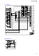
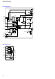
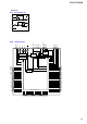
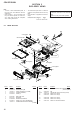
• IC Pin Function Description
MAIN BOARD IC501 R5F3650KBDZ85FA (SYSTEM CONTROLLER)
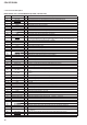
Pin No. Pin Name I/O Description
1 LCD_SO O Serial data output to the liquid crystal display driver
2 LCD_CLK O Serial data transfer clock signal output to the liquid crystal display driver
3
NOSE_SW I Front panel remove/attach detection switch input terminal “L”: front panel is attached
4 SIRCS I SIRCS signal input from the remote control receiver
5 UNISO O Serial data output to the bus interface
6 UNISI I Serial data input from the bus interface
7 UNISCK O Serial data transfer clock signal output to the bus interface
8 BYTE I External data bus width selection signal input terminal
9 CNVSS I Processor mode selection signal input terminal
10 XIN I Sub system clock signal input terminal (32.768 kHz)
11 XOUT O Sub system clock signal output terminal (32.768 kHz)
12
RESET I
System reset signal input from the reset signal generator and RESET switch “L”: reset
For several hundreds msec. after the power supply rises, “L” is input, then it change to “H”
13 OSCOUT O Main system clock signal output terminal (7.92 MHz)
14 VSS - Ground terminal
15 OSCIN I Main system clock signal input terminal (7.92 MHz)
16 VCC1 - Power supply terminal (+3.3V)
17
NMI I Non-maskable interrupt signal input terminal Fixed at “H” in this unit
18
RC_IN1 I Rotary commander shift key signal input terminal
19 BUIN I Back-up power detection signal input from the bus interface
20
SYSRST O System reset signal output to the CD mechanism deck block “L”: reset
21
BUS_ON O VBUS power control signal output to the bus interface
22 MC_RX I Serial data input from the CD mechanism deck block
23 DOOR_SW I Front panel open/close detection switch input terminal “L”: front panel is closed
24 MC_TX O Serial data output to the CD mechanism deck block
25 DOOR_ING O LED drive signal output terminal for disc slot indicator “H”: LED on
26 SYNC_OUT O Frequency control signal output to the USB VBUS power control
27 EJECT_OK O Eject OK signal output to the CD mechanism deck block
28 BEEP O Beep signal output to the power amplifi er
29 I2C_SCK O
IIC communication serial clock signal output to the PLL, power amplifi er and electrical
volume
30 I2C_SIO I/O
IIC communication serial data input/output with the PLL, power amplifi er and electrical
volume
31 FW_TXD O Serial data output terminal for fl ash writing
32 FW_RXD I Serial data input terminal for fl ash writing
33 FW_CLK I Serial clock signal input terminal for fl ash writing
34 FW_BUSY O Busy signal output terminal for fl ash writing
35, 36 NCO O Not used
37 CD_ON I CD mechanism servo power control request signal input from the CD mechanism deck block
38 CDM_ON I CD mechanism deck power control request signal input from the CD mechanism deck block
39 WAKE_UP O Wake-up signal output to the CD mechanism deck block
40 Z_MUTE I Zero detection muting signal input from the CD mechanism deck block
41 EPM O EPM signal output terminal Not used
42 MODELNAME_SEL0 I Model name selection signal input terminal Fixed at “L” in this unit
43 MODELNAME_SEL1 I Model name selection signal input terminal Fixed at “H” in this unit
44 MODELNAME_SEL2 I Model name selection signal input terminal Fixed at “L” in this unit
45 MODELNAME_SEL3 I Model name selection signal input terminal Fixed at “H” in this unit
46 CE O Chip enable signal output terminal Not used
47 NCO O Not used
48 SA_DATAIN I Spectrum analyzer serial data input from the CD mechanism deck block
49 SA_CLKOUT O Spectrum analyzer serial clock signal output to the CD mechanism deck block
50 USBON O USB power control signal output to the USB VBUS power control
51 VBUS_ON I
VBUS power control request signal input from the CD mechanism deck block
“H”: VBUS on
52
USB_OVR I USB over current detection signal input from the USB VBUS power control
53
EXTATT_XEN O Not used
54 NCO O Not used