
Product data

PCF8534A All information provided in this document is subject to legal disclaimers. © NXP B.V. 2011. All rights reserved.
Product data sheet Rev. 6 — 25 July 2011 26 of 52
NXP Semiconductors
PCF8534A
Universal LCD driver for low multiplex rates
8. Characteristics of the I
2
C-bus
The I
2
C-bus is for bidirectional, two-line communication between different ICs or modules.
The two lines are a Serial DAta Line (SDA) and a Serial CLock line (SCL). Both lines must
be connected to a positive supply via a pull-up resistor when connected to the output
stages of a device. Data transfer may be initiated only when the bus is not busy.
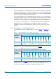
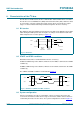
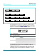
8.1 Bit transfer
One data bit is transferred during each clock pulse. The data on the SDA line must remain
stable during the HIGH period of the clock pulse as changes in the data line at this time
will be interpreted as a control signal (see Figure 14
).
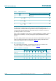
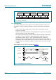
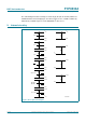
8.2 START and STOP conditions
Both data and clock lines remain HIGH when the bus is not busy.
A HIGH-to-LOW change of the data line, while the clock is HIGH, is defined as the START
condition (S).
A LOW-to-HIGH change of the data line, while the clock is HIGH, is defined as the STOP
condition (P).
The START and STOP conditions are illustrated in Figure 15
.
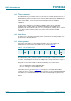
8.3 System configuration
A device generating a message is a transmitter, a device receiving a message is the
receiver. The device that controls the message is the master; and the devices which are
controlled by the master are the slaves. The system configuration is shown in Figure 16
.
Fig 14. Bit transfer
mba607
data line
stable;
data valid
change
of data
allowed
SDA
SCL
Fig 15. Definition of START and STOP conditions
mbc622
SDA
SCL
P
STOP condition
SDA
SCL
S
START condition