
Product data


PCF8534A All information provided in this document is subject to legal disclaimers. © NXP B.V. 2011. All rights reserved.
Product data sheet Rev. 6 — 25 July 2011 31 of 52
NXP Semiconductors
PCF8534A
Universal LCD driver for low multiplex rates
10. Limiting values
[1] Pins SDA, SCL, CLK, SYNC, SA0, OSC, and A0 to A2.
[2] Pins S0 to S59 and BP0 to BP3.
[3] Pass level; Human Body Model (HBM), according to Ref. 5 “
JESD22-A114”.
[4] Pass level; Charged-Device Model (CDM), according to Ref. 6 “
JESD22-C101”.
[5] Pass level; latch-up testing according to Ref. 7 “
JESD78” at maximum ambient temperature (T
amb(max)
).
[6] According to the NXP store and transport requirements (see Ref. 9 “
NX3-00092”) the devices have to be
stored at a temperature of +8 C to +45 C and a humidity of 25 % to 75 %. For long-term storage products
deviant conditions are described in that document.
CAUTION
Static voltages across the liquid crystal display can build up when the LCD supply voltage
(V
LCD
) is on while the IC supply voltage (V
DD
) is off, or vice versa. This may cause unwanted
display artifacts. To avoid such artifacts, V
LCD
and V
DD
must be applied or removed together.
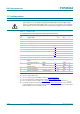
Table 18. Limiting values
In accordance with the Absolute Maximum Rating System (IEC 60134).
Symbol Parameter Conditions Min Max Unit
V
DD
supply voltage 0.5 +6.5 V
I
DD
supply current 50 +50 mA
V
LCD
LCD supply voltage 0.5 +7.5 V
I
DD(LCD)
LCD supply current 50 +50 mA
I
SS
ground supply current 50 +50 mA
V
I
input voltage
[1]
0.5 +6.5 V
I
I
input current
[1]
10 +10 mA
V
O
output voltage
[1]
0.5 +6.5 V
[2]
0.5 +7.5 V
I
O
output current
[1][2]
10 +10 mA
P
tot
total power dissipation - 400 mW
P/out power dissipation per
output
-100mW
V
ESD
electrostatic discharge
voltage
HBM
[3]
- 3000 V
CDM
[4]
- 1000 V
I
lu
latch-up current
[5]
-200mA
T
stg
storage temperature
[6]
65 +150 C
T
amb
ambient temperature operating device 40 +85 C