page 1/35 Direction des Recherches et des Développements VELIZY R&D Center Etablissement de VELIZY NOTE D'ETUDE / TECHNICAL DOCUMENT REFERENCE ETUDE / PROJECT URD1 – OTL 5665.1– 002 / NOM DE L’ETUDE 70 884 Code C TA1 HiloNC Module TITRE / TITLE : HiloNC Application note Edition Approbations /Approvals N° Rédacteur(s) Chef de projet # Author(s) J.DUMONT 03 Nom Name Date Chef Unité Project design manager Responsable d’entité / Product design manager T. Fu M. Boutboul E.
page 2/35 Direction des Recherches et des Développements VELIZY R&D Center Etablissement de VELIZY NOTE D'ETUDE / TECHNICAL DOCUMENT FICHE RECAPITULATIVE / SUMMARY SHEET Ed Date Date 1 27/06/2008 2 07/10/2008 3 10/11/2008 Référence Reference URD1– OTL 5665.1– 002 / 70 884 URD1– OTL 5665.1– 002 / 70 884 URD1– OTL 5665.1– 002 / 70 884 Rédacteur(s) Relecteur(s) Author(s) Steven Long Bingming Chen AMMARI. M. Reviser(s) Tiejun Fu / M. Boutboul DUMONT J. AMMARI M. Dumont J.
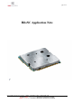
page 3/35 HiloNC Application Note Note d’étude / Technical document : URD1– OTL 5665.1– 002 / 70 884 Edition 03 Document Sagem Communications Reproduction et divulgation interdites Sagem Communications document.
page 4/35 Direction des Recherches et des Développements VELIZY R&D Center Etablissement de VELIZY SOMMAIRE / CONTENTS Direction des Recherches et des Développements Etablissement de VELIZY ................................................................1 NOTE D'ETUDE / TECHNICAL DOCUMENT.................................................................................................................1 Direction des Recherches et des Développements Etablissement de VELIZY ...................................
page 5/35 6.4 MECHANICAL SURROUNDING .....................................................................................................................26 6.5 OTHER RECOMMENDATIONS – TESTS FOR PRODUCTION/DESIGN ...............................................26 7. AUDIO INTEGRATION .............................................................................................................................................26 7.1 MECHANICAL INTEGRATION AND ACOUSTICS ...........................................
page 6/35 FIGURES LIST Figure 1: Block diagram of HiloNC module.............................................................................................................................8 Figure 2: SIM Card signals.....................................................................................................................................................10 Figure 3: Protections: EMC and ESD components close to the SIM................................................................................
page 7/35 1. OVERVIEW 1.1 OBJECT OF THE DOCUMENT The aim of this document is to describe some examples of hardware solutions for developing some products around the Sagem Communications HiloNC GPRS Module. Most part of these solutions is not mandatory. Use them as suggestions of what should be done to have a working product and what should be avoided thanks to our experiences.
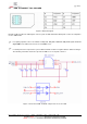
page 8/35 2.
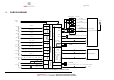
page 9/35 3. FUNCTIONAL INTEGRATION The improvement of Silicon technologies heads toward functionality improvement, less power consumption. The HiloNC module meets all these requirement and use last high end technology. among the 51 pads are in 2.8V domain which is suitable for most systems except : All digital- I/Os VSIM (the SIM I/Os at 1.8V or 2.9V) - VBAT (from 3.2V to 4.5V). Note d’étude / Technical document : URD1– OTL 5665.
page 10/35 3.1 HOW TO CONNECT TO A SIM CARD Figure 2: SIM Card signals HiloNC module provides the SIM signals on the 51 pads. A SIM card holder with 6 pads needs to be adopted to use the SIM function. Decoupling capacitors have to be added on SIM_CLK, SIM_RST, VSIM and SIM_DATA signals as close as possible to the SIM card connector to avoid EMC issues. Use ESD protection components to protect SIM card and module I/Os against Electro Static Discharges.
page 11/35 3.2 HOW TO CONNECT THE AUDIOS? The HiloNC module features one input audio path and one output audio path. The input path is single-end while the output path is differential. In this following chapter examples of design will be given including protections against EMC and ESD and some notes about the routing rules to follow to avoid the TDMA noise usually present in this sensitive area of design.
page 12/35 Ferrite Bead INTMIC_P HiloNC MIC 18pF ESD protection Figure 5 : Filter and ESD protection of microphone 3.2.1.2 Notes for speaker As explained for the microphone, if the speaker is deported out of the board or is sensitive to ESD, use the schematic here after to improve the audio.
page 13/35 3.2.2.1 Recommended characteristics for the microphone Item to be inspected Sensitivity Acceptance criterion - 40 dB SPL +/-3 dB (0 dB = 1 V/Pa @ 1kHz) Frequency response Limits (relatives values) Freq. (Hz) Lower limit 100 -1 200 -1 300 -1 1000 0 2000 -1 3000 -1.5 3400 -2 4000 -2 Upper limit 1 1 1 0 1 1.
page 14/35 note available PWM frequencies are too high to be used to make LEDs blinking. If purpose is to Please make LEDs blinking (for network states indication for example), GPIO usage is more accurate. 3.3.2 PWM for Buzzer connection The HiloNC module can manage a dedicate PWM output to drive a buzzer. The buzzer can be used to alarm for abnormal state. Resistors should be added to protect the buzzer. The value of these resistors depends on the buzzer and the transistor.
page 15/35 3.5 EXAMPLE OF POWER SUPPLY 3.5.1 Example 1 It the following application note from Linear Technology LTC3440, this schematic is an example of a DC/DC power supply able to power 3.6V under 2.1A. This can be use with a AC/DC 5V unit or an USB or PCMCIA bus as input power source. Figure 9: Example of power supply based on a DC/DC step down converter 3.5.
page 16/35 3.5.3 Example 3 Simple boost converter with Linear LT1913 (see LT1316 evaluation kit document). Figure 11: Example with Linear LT1913 3.6 V24 The HiloNC module features a V24 interface to communicate with the Host through AT commands or for easy firmware upgrading purpose. It is recommended to manage an external access to the V24 interface, in order to allow easy software upgrade (baud rate up to 460.8kbps, validated with ATEN USB/Serial converter).
page 17/35 HiLoNC Module 39 40 33 34 35 36 38 37 DTE Device RXD CTS DSR DCD RI DTR TXD RTS TXD CTS DSR DCD RI DTR RXD RTS 2.8V signals 2.8V signals Note: GND is not represented DCE point of view DTE point of view Figure 12: Complete V24 connection between HiloNC and host 3.6.2 Complete V24 interface with PC It supports speeds up to 115.2 Kbps and may be used in auto bauding mode. To use the V24 interface, some adaptation components are necessary to convert the +2.
page 18/35 Figure 14: Example of a connection to a data cable 3.6.3 Partial V24 (RX-TX-RTS-CTS) – connection HiloNC - host When using only RX/TX/RTS/CTS instead of the complete V24 link, we recommend following schematic. HiLoNC Module 39 40 33 34 35 36 38 37 DTE Device RXD CTS DSR DCD RI DTR TXD RTS TXD CTS DSR DCD RI DTR RXD RTS 2.8V signals Note: GND is not represented 2.
page 19/35 3.6.4 Partial V24 (RX-TX) – connection HiloNC - host When using only RX/TX instead of the complete V24 link, we recommend following schematic. HiLoNC Module 39 40 33 34 35 36 38 37 DTE Device RXD CTS DSR DCD RI DTR TXD RTS TXD CTS DSR DCD RI DTR RXD RTS 2.8V signals 2.
page 20/35 3.8 GPIO There are five GPIOs available on HiloNC. The GPIO1, GPIO2 and GPIO3 have internal pull-up resistors while GPIO4 and GPIO5 are open collector. GPIO4 and GPIO5 are used as output, they must be pulled up to VGPIO. The typical value of the pull-up Ifresisters is 100K ohms. 3.9 BACKUP BATTERY 3.9.1 Backup battery function feature 3.9.1.
page 21/35 R VBACKUP HiloNC Figure 17: Backup battery internally charged The resistor R depends on the charging current value provided by the battery manufacturer. The charging curve which is done by the HiloNC is given hereafter: Figure 18: Charging curve of backup battery 3.9.4 Backup Battery technology recommended 3.9.4.
page 22/35 Moreover, this kind of battery is available in the same kind of package than the Lithium Ion cell and fully compatible on a mechanical point of view. The only disadvantage is that the capacity of this kind of battery is significantly smaller than Manganese Silicon Lithium Ion battery. But for this kind of use (supply internal RTC when the main battery is removed), the capacity is generally enough. Sagem Communications strongly recommends using this kind of backup battery technology. 3.
page 23/35 When AT+KSLEEP=1 is configured : • the HiloNC module decides by itself when it enters in sleep mode (no more task running). • “0x00” character on serial link wakes up the HiloNC module. When AT+KSLEEP=0 is configured : • the HiloNC module is active when DTR signal is active (low electrical level). • when DTR is deactivated (high electrical level), the HiloNC module enters in sleep mode after a while. • on DTR activation (low electrical level), the HiloNC module wakes up.
page 24/35 4. MANDATORY POINTS FOR THE FINAL TESTS AND TUNING The design of the customer’s board (on which the module is soldered) must provide an access to following signals when the final product will be completely integrated. To upgrade the module software, Sagem Communications recommends providing a direct access to the module serial link through an external connector or any mechanism allowing the upgrade of the module without opening the whole product.
page 25/35 6. RADIO INTEGRATION 6.1 ANTENNA - Antenna contact • 50Ω line matching (between module and customer’s board, and with RF test point) Figure 20: Antenna connection Keep matching circuit on customer’s board but with direct connection in the first step – it could be necessary to make some adjustment later, during RF qualification stage. selected antenna must comply with FCC RF exposure limits in GSM850 and PCS1900 band : - TheGSM850 : MPE < 0.55mW/cm (Distance is 20 cm) 2 - 6.
page 26/35 Figure 21: Forbidden area for via and lines 6.4 MECHANICAL SURROUNDING Avoid any metallic part around the antenna area Keep jacks, FPCs and battery contact far from antenna area (FLEX) FPC has to be a shielded one 6.
page 27/35 To get a better audio output design (speaker part) : The speaker must be completely sealed on front side. The front aperture must be compliant with speaker supplier’s specifications The back volume must be completely sealed. The sealed back volume must be compliant with speaker supplier’s specifications Take care of the design of the speaker gasket (elastomer). Foresee a stable and large enough area for the gasket of the artificial ear.
page 28/35 8. RECOMMENDATIONS ON LAYOUT OF CUSTOMER’S BOARD 8.1 GENERAL RECOMMENDATIONS ON LAYOUT There are many different types of signals in the module which are disturbing each other. Particularly, Audio (1). signals are very sensitive to external signals as VBAT ... Therefore it is very important to respect some rules to avoid disruptions or abnormal behaviour. 8.1.
page 29/35 GND HSET_OUT_P HSET_OUT_N GND Figure 22: Layout of audio differential signals on a layer n GND Layer n-1 Layer n HSET_OUT_P Layer n+1 GND Figure 23: Adjacent layers of audio differential signals (1). Warning: Magnetic field generated by VBAT tracks may disturb the speaker, causing audio burst noise. In this case, one shall modify routing of the VBAT tracks to reduce the phenomena. 8.
page 30/35 Level 3 Floor Life Time 168 hours Conditions <= 30°C/60% RH Soak requirements Standard Accelerated Equivalent Time (hours) Conditions Time (hours) Conditions 192 +5/-0 30°C / 60% RH 40 +1/-0 60°C / 60%RH It means that the customer’s factory must process and solder the HiloNC on the customer’s board at least 168 hours (7 days) after the HiloNC sealed package have been opened. This duration is given for factory floor conditions of T°<30°C, HR 60%.
page 31/35 Note d’étude / Technical document : URD1– OTL 5665.1– 002 / 70 884 Edition 03 Document Sagem Communications Reproduction et divulgation interdites Sagem Communications document.
page 32/35 9.3 SOLDER MASK Below are given soldering characteristics to report the HiloNC on the customer’s board. Copper footprint is shown in yellow on the figure below. Solder mask footprint is shown in pink. Please note that copper mask and solder mask do not strictly recover themselves. Figure 25 : Solder mask design 9.4 SOLDER PASTE Solder paste : Alloy composition : Melting temperature : M705-GRN360-K-V (Senju Metal Industry Co., Ltd.) Sn96.5-Ag3.0-Cu0.
page 33/35 Figure 26 : Typical thermal profile The HiloNC module is a Lead-free product which has been validated integrated in a lead-free product, using a lead-free factory process. test has been performed using a leaded process. Sagem Communication does not recommend to use a factory leaded process and does not guarantee any No reliable result on the final product. Note d’étude / Technical document : URD1– OTL 5665.
page 34/35 9.6 SMT MACHINE HiloNC is optimized for use with pick-and-place machines.Optical inspection for placement is possible with SMD fiducials placed on the bottom side of the HiloNC. SMD fiducials are not symmetrical in order to help optical inspection to define the right orientation. Figure 27 : CMS fiducials positions 9.7 UNDERFILL Despite its important reliability, some customer could request for some specific and extreme applications the underfill of onboard components.
page 35/35 Underfill Holes Figure 28 : Underfill holes 9.8 SECOND REFLOW SOLDERING Even if Sagem Communications recommends a single reflow soldering, a second reflow soldering can be conceivable (only if underfill has not been already performed). Positive tests have been performed with HiloNC on the bottom side. Second reflow soldering is not possible if HiloNC module has been already underfilled. 9.9 HAND SOLDERING Hand soldering is possible. 9.